


 It’s Only Common Sense: The Phone Is Still Mightier Than the Keyboard
 The Marketing Minute: Marketing With Layers


Small Device That Bends Light to Generate New Radiation
October 25, 2018 | University of MichiganEstimated reading time: 3 minutes
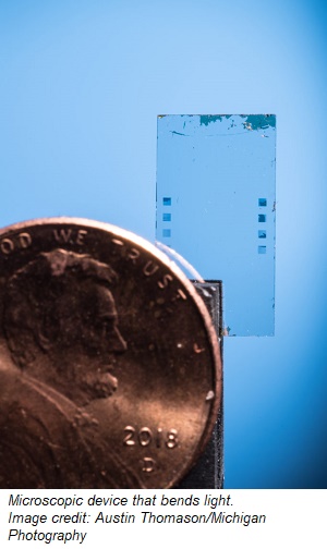
University of Michigan physicists have led the development of a device the size of a match head that can bend light inside a crystal to generate synchrotron radiation in a lab.
When physicists bend very intense beams of charged particles in circular orbits near the speed of light, this bending throws off bits of light, or X-rays, called synchrotron radiation. The U-M-led researchers used their device to bend visible light to produce light with a wavelength in the terahertz range. This range of wavelength is considerably larger than that of visible light, but much smaller than the waves your microwave produces—and can penetrate clothing.
Synchrotron radiation is usually generated at large-scale facilities, which are typically the size of several football stadiums. Instead, U-M researchers Roberto Merlin and Meredith Henstridge’s team developed a way to produce synchrotron radiation by printing a pattern of microscopic gold antennae on the polished face of a lithium tantalate crystal, called a metasurface. The U-M team, which also included researchers from Purdue University, used a laser to pulse light through the pattern of antennae, which bent the light and produced synchrotron radiation.
A research team led by University of Michigan physicists have developed a way to generate synchrotron using a device the size of a match head. Typically, synchrotron radiation is generated at facilities the size of several football fields. Image credit: Austin Thomason/Michigan Photography
“Instead of using lenses and spatial light modulators to perform this kind of experiment, we figured out by simply patterning a surface with a metasurface, you can achieve a similar end,” said Merlin, professor of physics and electrical engineering and computer science. “In order to get light to curve, you have to sculpt every piece of the light beam to a particular intensity and phase, and now we can do this in an extremely surgical way.”
Anthony Grbic, U-M professor of electrical engineering and computer science, led the team that designed the metasurface with former doctoral student Carl Pfeiffer developing the metasurface.
The metasurface is composed of roughly 10 million tiny boomerang-shaped antennae. Each antenna is considerably smaller than the wavelength of the impinging light, said Henstridge, lead author of the study. The researchers use a laser that produces “ultrashort” bursts or pulses of light which last for one trillionth of a second. The array of antennae causes the light pulse to accelerate along a curved trajectory inside the crystal.
The light pulse creates a collection of electric dipoles—or, a group of positive and negative charge pairs. This dipole collection accelerates along the curved trajectory of the light pulse, resulting in the emission of synchrotron radiation, according to Henstridge, who earned her doctoral degree at U-M and is now a postdoctoral scientist at the Max Planck Institute for the Structure and Dynamics of Matter in Hamburg, Germany.
The researchers’ device produces synchrotron radiation that contains many terahertz frequencies because the light pulses travel just a fraction of a circle. But they hope to refine their device so that the light pulse revolves continuously along a circular path, producing synchrotron radiation at a single terahertz frequency.
The scientific community uses single-frequency terahertz sources to study the behavior of atoms or molecules within a given solid, liquid or gas. Commercially, terahertz sources are used to scan items hidden in clothing and packaging crates. Drugs, explosive and toxic gases all have unique “fingerprints” in the terahertz range that could be identified using terahertz spectroscopy.
The device’s uses aren’t limited to the security industry.
“Terahertz radiation is useful for imaging in the biomedical sciences,” Henstridge said. “For instance, it has been used to distinguish between cancerous and healthy tissue. An on-chip, single-frequency terahertz source, such as a tiny light-driven synchrotron such as our device, can allow for new advancements in all of these applications.”
Share on:


Testimonial
"In a year when every marketing dollar mattered, I chose to keep I-Connect007 in our 2025 plan. Their commitment to high-quality, insightful content aligns with Koh Young’s values and helps readers navigate a changing industry. "
Brent Fischthal - Koh YoungSuggested Items
Smart Eye Collaborates with Sony on Next-Generation Interior Sensing and Iris Authentication
10/09/2025 | Smart EyeSmart Eye AB, the global leader in Interior Sensing AI and Driver Monitoring Systems (DMS), announced a collaboration with Sony Semiconductor Solutions Corporation (Sony) to integrate Smart Eye’s interior sensing and biometric authentication software with Sony’s newly released IMX775 RGB-IR image sensor.
SEMICON Europa 2025 to Highlight Innovations in Advanced Packaging, Fab Management, and MEMS and Imaging Sensors to Bolster Europe’s Semiconductor Resilience
10/03/2025 | SEMISemiconductor industry experts will convene at SEMICON Europa 2025, November 18-21 at Messe München in Munich, to explore the latest trends and innovations in advanced packaging and fab management.
MEMS & Imaging Sensors Summit to Spotlight Sensing Revolution for Europe’s Leadership
09/11/2025 | SEMIIndustry experts will gather November 19-20 at the SEMI MEMS & Imaging Sensors Summit 2025 to explore the latest breakthroughs in AI-driven MEMS and imaging optimization, AR/VR technologies, and advanced sensor solutions for critical defence applications.
Direct Imaging System Market Size to Hit $4.30B by 2032, Driven by Increasing Demand for High-Precision PCB Manufacturing
09/11/2025 | Globe NewswireAccording to the SNS Insider, “The Direct Imaging System Market size was valued at $2.21 Billion in 2024 and is projected to reach $4.30 Billion by 2032, growing at a CAGR of 8.68% during 2025-2032.”
I-Connect007’s Editor’s Choice: Five Must-Reads for the Week
07/04/2025 | Marcy LaRont, I-Connect007For our industry, we have seen several bullish market announcements over the past few weeks, including one this week by IDC on the massive growth in the global server market. We’re also closely watching global trade and nearshoring. One good example of successful nearshoring is Rehm Thermal Systems, which celebrates its 10th anniversary in Mexico and the official opening of its new building in Guadalajara.