


 The Chemical Connection: Onshoring PCB Production—Daunting but Certainly Possible
 It’s Only Common Sense: The Phone Is Still Mightier Than the Keyboard


Gold 'Micro Jewels' from 3D Printer Printing Pure Metal Microparts
October 30, 2018 | University of TwenteEstimated reading time: 2 minutes
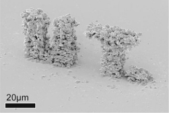
Thanks to a laser technique that ejects ultra-tiny droplets of metal, it is now possible to print 3D metal structures, not only simple ‘piles’ of droplets, but complex overhanging structures as well: like a helix of some microns in size, made of pure gold. Using this technique, it will be possible to print new 3D micro components for electronics or photonics.
By pointing an ultra-short laser pulse onto a nanometer thin metal film, a tiny metal droplet melts, it is ejected to its target and solidifies again after landing. Thanks to this technique, called laser-induced forward transfer (LIFT), the UT researchers are able to build, drop by drop, a structure with copper and gold microdroplets. The copper acts as a mechanical support for the gold. In their paper in Additive Manufacturing the researchers show, for example, a printed helix: this could act as a mechanical spring or an electric inductor at the same time. This helix is printed with copper around it: together with the helix, a copper ‘box’ is printed. In this way, a droplet that is meant for the new winding that is printed, is prevented from landing on the previous winding. After building the helix, drop by drop and layer by layer, the copper support box is etched away chemically. What remains is a helix of pure gold, no more than a few tens of microns in size.
The laser printing technique: by printing copper and gold in turn, the gold helix initially is surrounded by a copper box. Etching the copper away, results in a free standing helix of pure gold.
Top view (c) of the helix shows that it is threedimensional with a center void. In (b), it is still in the copper box
No Mixing
The volume of the metal droplets is a few femtoliters: a femtoliter is 10-15 liter. To give an impression, a femtoliter droplet has a diameter of little over one micrometer. The way the droplets are made, is by lighting the metal using an ultrashort pulse of green laser light. In this way, the copper and gold structure is built. A crucial question for the researchers was if the two metals would mix at their interface: this would have consequences for the quality of the product after etching. Research shows that there isn’t any mixing. The way a structure is built, drop by drop, results in a surface roughness, which is only about 0.3 to 0.7 microns.
Biomedical
The LIFT technique is a promising technique for other metals and combinations of metals as well. The researchers expect opportunities for materials used in 3D electronic circuit, micromechanic devices and sensing in, for example, biomedical applications. It therefore is a powerful new production technique on a very small scale: an important step towards ‘functionalisation’ of 3D printing.
The research published now, has been done by the departments of Mechanics of Solids, Surfaces and Systems (MS3) and Design, Production and Management (DPM), both part of the Engineering Technology faculty of the University of Twente. The researchers collaborated with DEMCON corporation, a spinoff company of the University of Twente.
Share on:


Testimonial
"The I-Connect007 team is outstanding—kind, responsive, and a true marketing partner. Their design team created fresh, eye-catching ads, and their editorial support polished our content to let our brand shine. Thank you all! "
Sweeney Ng - CEE PCBSuggested Items
Episode 6 of Ultra HDI Podcast Series Explores Copper-filled Microvias in Advanced PCB Design and Fabrication
10/15/2025 | I-Connect007I-Connect007 has released Episode 6 of its acclaimed On the Line with... American Standard Circuits: Ultra High Density Interconnect (UHDI) podcast series. In this episode, “Copper Filling of Vias,” host Nolan Johnson once again welcomes John Johnson, Director of Quality and Advanced Technology at American Standard Circuits, for a deep dive into the pros and cons of copper plating microvias—from both the fabricator’s and designer’s perspectives.
Nolan’s Notes: Tariffs, Technologies, and Optimization
10/01/2025 | Nolan Johnson -- Column: Nolan's NotesLast month, SMT007 Magazine spotlighted India, and boy, did we pick a good time to do so. Tariff and trade news involving India was breaking like a storm surge. The U.S. tariffs shifted India from one of the most favorable trade agreements to the least favorable. Electronics continue to be exempt for the time being, but lest you think that we’re free and clear because we manufacture electronics, steel and aluminum are specifically called out at the 50% tariff levels.
MacDermid Alpha & Graphic PLC Lead UK’s First Horizontal Electroless Copper Installation
09/30/2025 | MacDermid Alpha & Graphic PLCMacDermid Alpha Electronics Solutions, a leading supplier of integrated materials and chemistries to the electronics industry, is proud to support Graphic PLC, a Somacis company, with the installation of the first horizontal electroless copper metallization process in the UK.
Electrodeposited Copper Foils Market to Grow by $11.7 Billion Over 2025-2032
09/18/2025 | Globe NewswireThe global electrodeposited copper foils market is poised for dynamic growth, driven by the rising adoption in advanced electronics and renewable energy storage solutions.
MacDermid Alpha Showcases Advanced Interconnect Solutions at PCIM Asia 2025
09/18/2025 | MacDermid Alpha Electronics SolutionsMacDermid Alpha Electronic Solutions, a global leader in materials for power electronics and semiconductor assembly, will showcase its latest interconnect innovations in electronic interconnect materials at PCIM Asia 2025, held from September 24 to 26 at the Shanghai New International Expo Centre, Booth N5-E30