


 Trouble in Your Tank: Implementing Direct Metallization in Advanced Substrate Packaging
 It’s Only Common Sense: Storytelling That Sells—Stop Pitching, Start Painting Pictures
 The Right Approach: Get Ready for ISO 9001 Version 6


Tests Show Integrated Quantum Chip Operations Possible
October 30, 2018 | UNSW SydneyEstimated reading time: 5 minutes
Two fundamental quantum techniques have been combined by a UNSW team in a integrated silicon chip for the first time, confirming the promise of using silicon for quantum computing.
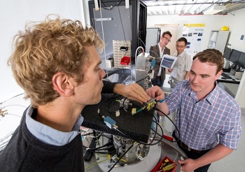
Image Caption: Dzurak’s team at UNSW, who conducted the experiments. From Left to Right: Dr Bas Hensen, Prof Dzurak, Dr Kok Wai Chan, and former PhD student Michael Fogarty, who was lead author on the paper. (Photo: Paul Henderson-Kelly)
Quantum computers that are capable of solving complex problems, like drug design or machine learning, will require millions of quantum bits – or qubits – connected in an integrated way and designed to correct errors that inevitably occur in fragile quantum systems. Now, an Australian research team has experimentally realised a crucial combination of these capabilities on a silicon chip, bringing the dream of a universal quantum computer closer to reality.
They have demonstrated an integrated silicon qubit platform that combines both single-spin addressability – the ability to ‘write’ information on a single spin qubit without disturbing its neighbours – and a qubit ‘read-out’ process that will be vital for quantum error correction. Moreover, their new integrated design can be manufactured using well-established technology used in the existing computer industry.
The team is led by Scientia Professor Andrew Dzurak of UNSW Sydney, a program leader at the Centre of Excellence for Quantum Computation and Communication Technology (CQC2T) and Director of the NSW node of the Australian National Fabrication Facility.
Last year, Dzurak and colleagues published a design for a novel chip architecture that could allow quantum calculations to be performed using silicon CMOS (complementary metal-oxide-semiconductor) components – the basis of all modern computer chips.
In their new study, published today in the journal Nature Communications, the team combine two fundamental quantum techniques for the first time, confirming the promise of their approach.
Dzurak’s team had also previously shown that an integrated silicon qubit platform can operate with single-spin addressability – the ability to rotate a single spin without disturbing its neighbours.
They have now shown that they can combine this with a special type of quantum readout process known as Pauli spin blockade, a key requirement for quantum error correcting codes that will be necessary to ensure accuracy in large spin-based quantum computers. This new combination of qubit readout and control techniques is a central feature of their quantum chip design.
“We’ve demonstrated the ability to do Pauli spin readout in our silicon qubit device but, for the first time, we've also combined it with spin resonance to control the spin,” says Dzurak.
“This is an important milestone for us on the path to performing quantum error correction with spin qubits, which is going to be essential for any universal quantum computer.”
Lead author Michael Fogarty, who performed the experiments as part of his PhD research with Professor Dzurak at UNSW, says: “Quantum error correction is a key requirement in creating large-scale useful quantum computing because all qubits are fragile, and you need to correct for errors as they crop up.”
But Fogarty notes this “creates significant overhead in the number of physical qubits you need in order to make the system work”.
Dzurak says: “By using silicon CMOS technology we have the ideal platform to scale to the millions of qubits we will need, and our recent results provide us with the tools to achieve spin qubit error-correction in the near future.
“It’s another confirmation that we’re on the right track. And it also shows that the architecture we’ve developed at UNSW has, so far, shown no roadblocks to the development of a working quantum computer chip – and, what’s more, one that can be manufactured using well-established industry processes and components.”
Page 1 of 2
Share on:


Testimonial
"The I-Connect007 team is outstanding—kind, responsive, and a true marketing partner. Their design team created fresh, eye-catching ads, and their editorial support polished our content to let our brand shine. Thank you all! "
Sweeney Ng - CEE PCBSuggested Items
United Electronics Corporation Unveils Revolutionary CIMS Galaxy 30 Automated Optical Inspection System
09/11/2025 | United Electronics CorporationUnited Electronics Corporation (UEC) today announced the launch of its new groundbreaking CIMS Galaxy 30 Automated Optical Inspection (AOI) machine, setting a new industry standard for precision electronics manufacturing quality control. The Galaxy 30, developed and manufactured by CIMS, represents a significant leap forward in inspection technology, delivering exceptional speed improvements and introducing cutting-edge artificial intelligence capabilities.
Intel Announces Key Leadership Appointments to Accelerate Innovation and Strengthen Execution
09/09/2025 | Intel CorporationIntel Corporation today announced a series of senior leadership appointments that support the company’s strategy to strengthen its core product business, build a trusted foundry, and foster a culture of engineering across the business.
DARPA, State of New Mexico Establish Framework to Advance Quantum Computing
09/08/2025 | DARPAAs part of the Quantum Benchmarking Initiative (QBI), DARPA signed an agreement with the State of New Mexico’s Economic Development Department to create the Quantum Frontier Project.
LPKF Strengthens LIDE Technology Leadership with New Patent Protection in Korea
09/04/2025 | LPKFLPKF Laser & Electronics SE today announced that its groundbreaking LIDE (Laser Induced Deep Etching) technology has received additional patent protection in Korea through the Korean Patent Office (KPCA), effective September 1, 2025.
UHDI Fundamentals: UHDI Technology and Industry 4.0
09/03/2025 | Anaya Vardya, American Standard CircuitsUltra high density interconnect (UHDI) technology is rapidly transforming how smart systems are designed and deployed in the context of Industry 4.0. With its capacity to support highly miniaturized, high-performance, and densely packed electronics, UHDI is a critical enabler of the smart, connected, and automated industrial future. Here, I’ll explore the synergy between UHDI and Industry 4.0 technologies, highlighting applications, benefits, and future directions.