-
-
News
News Highlights
- Books
Featured Books
- pcb007 Magazine
Latest Issues
Current IssueThe Hole Truth: Via Integrity in an HDI World
From the drilled hole to registration across multiple sequential lamination cycles, to the quality of your copper plating, via reliability in an HDI world is becoming an ever-greater challenge. This month we look at “The Hole Truth,” from creating the “perfect” via to how you can assure via quality and reliability, the first time, every time.
In Pursuit of Perfection: Defect Reduction
For bare PCB board fabrication, defect reduction is a critical aspect of a company's bottom line profitability. In this issue, we examine how imaging, etching, and plating processes can provide information and insight into reducing defects and increasing yields.
Voices of the Industry
We take the pulse of the PCB industry by sharing insights from leading fabricators and suppliers in this month's issue. We've gathered their thoughts on the new U.S. administration, spending, the war in Ukraine, and their most pressing needs. It’s an eye-opening and enlightening look behind the curtain.
- Articles
- Columns
- Links
- Media kit
||| MENU - pcb007 Magazine
Copper Pillar Plating Systems: High Speed, Low Heat
November 1, 2018 | E. Walch, DJ., C. Rietmann, Ph.D., and A. Angstenberger, Ph.D.Estimated reading time: 1 minute

Abstract
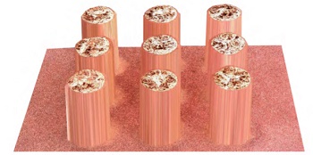
The industry is seeing ever-more stringent requirements of interconnect technologies (ICT) from die through final assembly, in particular digital and analog high frequencies, undistorted signal propagation and efficient heat propagation are concerned. From wafer level packaging to the finished printed circuit board, copper pillars, and solid copper posts (with printed circuitry it is copper filled through-holes, respectively) continue to play a vital role in coping with high-speed/high-frequency and high wattage of sub and final assemblies.
Commonly used packaging concepts comprising wafer level plating, through-silicon-vias (TSV), redistribution layer design (RDL), intermediate pillars, macrobumps and copper-filled through-holes in the final circuitry will be addressed in this article, followed by an overlook of the extremely different pillar geometries within each packaging level, posing individual challenges on the copper plating chemistry and process. Practical aspects, namely dialing in the chemistry additives and process windows to match the relevant applications‘ needs will be reported, as well as the ongoing R&D work targeted for current and future requirements. The article concludes with actual research results on achievable copper textures and the subsequent performance of the plated copper interconnects as far as crystal lattices and the related thermal reliability are concerned.
To read the full version of this article which originally appeared in the September 2018 issue of PCB007 magazine, click here.
Suggested Items
The Evolution of Picosecond Laser Drilling
06/19/2025 | Marcy LaRont, PCB007 MagazineIs it hard to imagine a single laser pulse reduced not only from nanoseconds to picoseconds in its pulse duration, but even to femtoseconds? Well, buckle up because it seems we are there. In this interview, Dr. Stefan Rung, technical director of laser machines at Schmoll Maschinen GmbH, traces the technology trajectory of the laser drill from the CO2 laser to cutting-edge picosecond and hybrid laser drilling systems, highlighting the benefits and limitations of each method, and demonstrating how laser innovations are shaping the future of PCB fabrication.
Day 2: More Cutting-edge Insights at the EIPC Summer Conference
06/18/2025 | Pete Starkey, I-Connect007The European Institute for the PCB Community (EIPC) summer conference took place this year in Edinburgh, Scotland, June 3-4. This is the third of three articles on the conference. The other two cover Day 1’s sessions and the opening keynote speech. Below is a recap of the second day’s sessions.
Day 1: Cutting Edge Insights at the EIPC Summer Conference
06/17/2025 | Pete Starkey, I-Connect007The European Institute for the PCB Community (EIPC) Summer Conference took place this year in Edinburgh, Scotland, June 3-4. This is the second of three articles on the conference. The other two cover the keynote speeches and Day 2 of the technical conference. Below is a recap of the first day’s sessions.
Preventing Surface Prep Defects and Ensuring Reliability
06/10/2025 | Marcy LaRont, PCB007 MagazineIn printed circuit board (PCB) fabrication, surface preparation is a critical process that ensures strong adhesion, reliable plating, and long-term product performance. Without proper surface treatment, manufacturers may encounter defects such as delamination, poor solder mask adhesion, and plating failures. This article examines key surface preparation techniques, common defects resulting from improper processes, and real-world case studies that illustrate best practices.
RF PCB Design Tips and Tricks
05/08/2025 | Cherie Litson, EPTAC MIT CID/CID+There are many great books, videos, and information online about designing PCBs for RF circuits. A few of my favorite RF sources are Hans Rosenberg, Stephen Chavez, and Rick Hartley, but there are many more. These PCB design engineers have a very good perspective on what it takes to take an RF design from schematic concept to PCB layout.