


 The Marketing Minute: If Your Marketing Budget Gets Cut in Half, Then What?
 Punching Out: How Are the Big Boys in Electronics Doing?
 It’s Only Common Sense: Complexity Is the Enemy of Profit


Ventec at electronica 2018: No Compromises for High-Frequency Materials
November 2, 2018 | Ventec International GroupEstimated reading time: 3 minutes
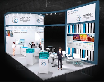
Ventec International Group will announce the launch of its extended ceramic-filled hydrocarbon thermoset material series designed for the world's most demanding high-frequency printed circuit board applications at this year’s electronica show in Munich. The global Ventec team will also be on hand in hall A1 at booth #468 to present the company’s unique laminate and prepreg capability across a very wide range of applications and budgets under the theme of ‘No more compromises: Price, Performance and Availability.'
From 13-16 November, electronica 2018 will be the global launch platform for Ventec's extended tec speed 20.0 range of ceramic-filled hydrocarbon thermoset material series. Combining unrivalled high-frequency performance (Dk 3.00-3.48/Df 0.002-0.0037), superior loss characteristics and the highest reliability with fast availability and efficient delivery through Ventec's fully controlled and managed global supply chain and technical support-network, the tec-speed 20.0 series offers excellent dimensional stability and uniform mechanical properties that help limit PIM. With the extended tec speed 20.0 range, Ventec has responded to customer demands for high-performance, reliable and cost-efficient high frequency materials that are supported by a fast and efficient global delivery promise and dependable technical support.
Other show highlights include:
Material Showcase
A special product & material showcase will demonstrate PCB material applications including a power module and a LED lighting module that illustrates examples of IMS boards combined with FR4 control boards made with Ventec’s high performance and highly reliable IMS materials like VT-4B5SP, VT-4B5L and VT-4B7. Automotive manufacturers around the world, including Ford, Tesla, VAG, Audi, Skoda, Seat, Volkswagen, Tata, Bentley, Daimler Benz, BMW, Renault-Nissan, Jaguar/Land Rover, Maclaren Automotive, already rely on Ventec's thermal management materials for a range of applications including LED headlights, ECU, break energy reclamation & e-power train establishing Ventec as a global leader in technology for high performance thermal management materials.
Announcing European Distribution Agreement for Thermal Interface Materials
As a perfect complement to Ventec’s IMS material families, thermally conductive and standard laminates and prepregs for multilayer PCB’s, Ventec has teamed up with EMI Thermal to provide a range of Thermal Interface Materials (TIM) to the European market. TIM is a thermally conductive medium used to fill the air gaps between mating surfaces in electronic components. Air is a poor conductor of heat and creates a thermal barrier which stops the transfer of heat between the component and its heatsink or chassis. EMI Thermal’s range of materials distributed through Ventec includes double sided thermal tape, electrical insulators, natural graphite and void fillers, that ensure reliability and performance and prevent electronic components from overheating and being damaged or burnt out.
With a one-stop-service solution for customers, Ventec also offers further distribution products to the European PCB and electronics industry including flexible laminates (ThinFlex/Arisawa) and a full range of PCB production consumable products covering standard and speciality (Centrum & Glossback) drill materials, copper foils including ACF.
Stock exchange Listing Celebration
Ventec is amid a transformative phase of its impressive history, having been successfully listed and trading on the Emerging Stock Market of the Taipei Stock Exchange since 16 January 2018 and currently completing the process for a TPEx Mainboard listing for early 2019. To celebrate the successful IPO as well as the launch of its latest product offerings, Ventec is looking forward to hosting show-visitors at its booth party on Wednesday, 14 November from 18:00 to 21:30.
About Ventec International Group
With volume manufacturing facilities and Headquarters in Suzhou China, Ventec International specializes in advanced copper clad glass reinforced and metal backed substrates for the PCB industry. With distribution locations and manufacturing sites in both the US and Europe, Ventec International is a premier supplier to the global PCB industry. For more information, click here.
Visit I-007eBooks to download your copy of Ventec micro eBook today:
The Printed Circuit Designer's Guide to...Thermal Management with Insulated Metal Substrates
Share on:


Testimonial
"Our marketing partnership with I-Connect007 is already delivering. Just a day after our press release went live, we received a direct inquiry about our updated products!"
Rachael Temple - AlltematedSuggested Items
I-Connect007 Releases The Printed Circuit Designer’s Guide to… Direct Metallization: A Guide to Complex PCB Fabrication
05/15/2026 | I-Connect007As PCB complexity continues to accelerate, fabricators and OEMs are reevaluating long-standing manufacturing processes to meet the demands of AI, HDI, advanced packaging, and next-generation electronics. To address these evolving challenges, I-Connect007 is proud to announce the release of The Printed Circuit Designer’s Guide to… Direct Metallization: A Guide to Complex PCB Fabrication, authored by MacDermid Alpha Solution’s Carmichael Gugliotti.
Driving Innovation: Selecting the Right Laser Source
04/28/2026 | Simon Khesin -- Column: Driving InnovationWhen I first joined Schmoll Maschinen, I brought experience from almost every PCB process, except for laser. As I immersed myself in laser processing, I realized why it can seem so daunting to a newcomer. The complexity arises from three intersecting factors: A vast variety of laser sources: CO2, UV-nano, green-pico, UV-pico, IR-pico, and others; a diverse range of applications: Drilling, cutting, ablation, and more; and an extensive list of materials: These have vastly different absorption rates. Choosing the right machine or laser source is rarely trivial. Even for experienced engineers, answering "Which source is best?" requires examining the business's specific goals.
Institute of Circuit Technology Spring Seminar 2026: A Bright Future in Europe
04/23/2026 | Pete Starkey, I-Connect007Through the leafy lanes and spring flowers of Warwickshire and back to Meridan, the traditional centre of England, and now officially part of the Metropolitan Borough of Solihull in the county of the West Midlands, I attended the Annual General Meeting and Spring Seminar of the Institute of Circuit Technology (ICT) on April 14. Out of the AGM came notable changes in leadership at the top of the Institute: the retirement of Mat Beadel as chair and Emma Hudson as technical director. Effective May 1, Steve Driver is the new chair, and Alun Morgan is the new technical director.
ACCM Unveils Negative and Near-zero CTE Materials for Large-Format AI Chips
04/21/2026 | Advanced Chip and Circuit MaterialsAdvanced Chip and Circuit Materials, Inc. (ACCM) has launched two new materials: Celeritas HM50, with a negative coefficient of thermal expansion (CTE) of -8 ppm/°C to offset the positive CTE and expansion of copper with temperature on circuit boards, and Celeritas HM001, with near-zero CTE and the low-loss performance needed for high-speed signal layers to 224 Gb/s and faster in artificial intelligence (AI) circuits.
Fresh PCB Concepts: Designing PCBs for Harsh Environments—Reliability Is Engineered Upstream
04/23/2026 | Team NCAB -- Column: Fresh PCB ConceptsWhen engineers hear the phrase “harsh environment,” they usually think of the extreme temperature swings, vibration and shock, pressure changes, or radiation in aerospace. However, aerospace is not the only harsh environment where electronic assemblies must survive. Automotive power electronics, downhole oil and gas tools, marine controls, rail systems, defense platforms, and industrial automation equipment all expose PCBs to environments that are equally unforgiving. The stress mechanisms may differ, but the physics does not.