


 Driving Innovation: Mechanical and Optical Processes During Rigid-flex Production
 It’s Only Common Sense: Your Biggest Competitor Is Complacency
 The Chemical Connection: Onshoring PCB Production—Daunting but Certainly Possible


Electronic Highways on the Nanoscale
November 2, 2018 | Technische Universität ChemnitzEstimated reading time: 2 minutes
For the first time, the targeted functionalization of carbon-based nanostructures allows the direct mapping of current paths, thereby paving the way for novel quantum devices.
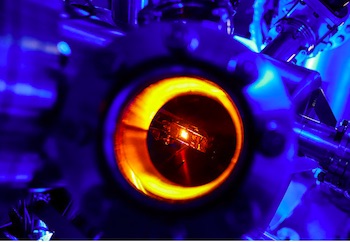
Image Caption: In the Laboratory of the Department of Analytics of Solid Surfaces at the Chemnitz University of Technology, a structured silicon carbide crystal is heated in a preparation chamber of a scanning tunneling microscope, so that small graphene structures can be formed. Photo: Jacob Müller
Computers are getting faster and increasingly powerful. However, at the same time computing requires noticeably more energy, which is almost completely converted to wasted heat. This is not only harmful to the environment, but also limits further miniaturization of electronic components and increase of clock rates. A way out of this dilemma are conductors with no electrical resistance. Based on carbon nanostructures, such conductors can be realized. By applying sophisticated heating processes to nanostructured silicon carbide crystals, small graphene structures, so-called graphene nanoribbons, can be produced at their edges. Graphene is a single layer of carbon atoms arranged in a honeycomb lattice.
Physicists at the Chemnitz University of Technology in collaboration with researchers from the University of Twente (Netherlands) and the MAX IV Laboratory in Lund (Sweden) succeeded now to produce and to characterize such so-called ballistic wires. "The intriguing property of such conductors is that the electrons pass through these tiny wires without heating them—ideally irrespective of the wire length," explains Prof. Dr. Christoph Tegenkamp, chair of the Department of Analytics of Solid Surfaces at the Chemnitz University of Technology. In a variety of complex experiments including atomic force and multi-tip scanning tunneling microscopy, the adjacent quantum transport channels were measured in detail and even imaged directly at room temperature and atmosphere on the nanoscale. "Surprisingly, we could now even identify several spatially separated channels on one wire that apparently do not influence each other," explains Johannes Aprojanz, who is currently working on this research topic at the Chemnitz University of Technology in his doctoral thesis.
In cooperation with theorists from Copenhagen and Barcelona, this unique effect has been traced back to an asymmetric interaction of the edges with the substrate, as reported in the journal Nature Communication in its current issue. The authors of the study are sure that this type of functionalization is also interesting for topological effects in other 2D materials and shows new ways for the design of future quantum devices. "We are opening the door a bit wider for computers that are hardly warming up," said Tegenkamp.
Share on:


Testimonial
"Advertising in PCB007 Magazine has been a great way to showcase our bare board testers to the right audience. The I-Connect007 team makes the process smooth and professional. We’re proud to be featured in such a trusted publication."
Klaus Koziol - atgSuggested Items
LPKF Delivers Key Strategic Technology to Fraunhofer's Glass Panel Technology Group
10/29/2025 | LPKFLPKF Laser & Electronics SE is one of the initiators of the Glass Panel Technology Group (GPTG), a consortium encompassing the entire process chain for advanced semiconductor packaging with glass substrates.
On the Line With… Ultra HDI Podcast—Episode 7: “Solder Mask: Beyond the Traces,” Now Available
10/29/2025 | I-Connect007I-Connect007 is excited to announce the release of the seventh episode of its 12-part podcast series, On the Line With… American Standard Circuits: Ultra HDI. In this episode, “Solder Mask: Beyond the Traces,” host Nolan Johnson sits down with John Johnson, Director of Quality and Advanced Technology at American Standard Circuits, to explore the essential role that solder mask plays in the Ultra HDI (UHDI) manufacturing process.
Nvidia’s Blackwell Chips Made in Arizona Still Head to Taiwan for Final Assembly
10/27/2025 | I-Connect007 Editorial TeamNvidia has begun production of its next-generation Blackwell GPUs in the United States, but the company still depends heavily on Taiwan to complete the process, The Register reported.
American Standard Circuits Launches 50th 77-Second Webinar
10/27/2025 | American Standard CircuitsAnaya Vardya, President and CEO of American Standard Circuits/ASC Sunstone Circuits is pleased to announce that they have recently unveiled their 50th 77-second webinar.
KYZEN Brings Reliability to Life at productronica 2025 with ANALYST² Process Control Demos
10/22/2025 | KYZEN'KYZEN, the global leader in innovative environmentally responsible cleaning chemistries, will exhibit at productronica 2025, November 18–21 in Munich, Germany, where the company will put a spotlight on its award-winning KYZEN ANALYST² process control system in Hall A4, Stand 450.