


 Driving Innovation: Mechanical and Optical Processes During Rigid-flex Production
 It’s Only Common Sense: Your Biggest Competitor Is Complacency
 The Chemical Connection: Onshoring PCB Production—Daunting but Certainly Possible


Detecting Light in a Different Dimension
November 14, 2018 | Brookhaven National LaboratoryEstimated reading time: 3 minutes
Scientists from the Center for Functional Nanomaterials (CFN)—a U.S. Department of Energy (DOE) Office of Science User Facility at Brookhaven National Laboratory—have dramatically improved the response of graphene to light through self-assembling wire-like nanostructures that conduct electricity.
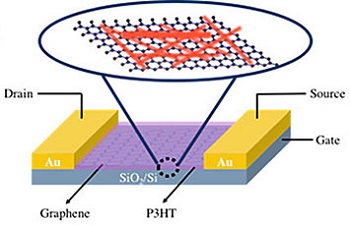
Image Caption: Cartoon of the graphene-P3HT nanowire hybrid field-effect transistor. Placing the nanowire mesh (red) on top of the graphene (purple) improves the device's response to light. The silicon dioxide/silicon (grey) substrate, or "gate" electrode, controls the flow of electrical current between the electron source and drain (in this case, Au, or gold, electrodes). The scientists used electron-beam lithography to pattern the device.
The improvement could pave the way for the development of graphene-based detectors that can quickly sense light at very low levels, such as those found in medical imaging, radiation detection, and surveillance applications.
Graphene is a two-dimensional (2-D) nanomaterial with unusual and useful mechanical, optical, and electronic properties. It is both extremely thin and incredibly strong, detects light of almost any color, and conducts heat and electricity well. However, because graphene is made of sheets of carbon only one atom thick, it can only absorb a very small amount of incoming light (about two percent).
One approach to overcoming this problem is to combine graphene with strong light-absorbing materials, such as organic compounds that conduct electricity. Scientists recently demonstrated an improved photoresponse by placing thin films (a few tens of nanometers) of one such conductive polymer, poly(3-hexylthiophene), or P3HT, on top of a single layer of graphene.
Now, the CFN scientists have improved the photoresponse by an additional 600% by changing the morphology (structure) of the polymer. Instead of thin films, they used a mesh of nanowires—nanostructures that are many times longer than they are wide—made of the same polymer and similar thickness. The research is described in an article published online on Oct. 12 in ACS Photonics, a journal of the American Chemical Society (ACS).
“We used self-assembly, a very simple and reproducible method, to create the nanowire mesh,” said first author Mingxing Li, a research associate in the CFN Soft and Bio Nanomaterials Group. “Placed in an appropriate solution and stirred overnight, the polymer will form into wire-like nanostructures on its own. We then spin-casted the resulting nanowires onto electrical devices called graphene field-effect transistors (FETs).”
The scientists fabricated FETs made of graphene only, graphene and P3HT thin films, and graphene and P3HT nanowires. After checking the thickness and crystal structure of the FET devices through atomic force microscopy, Raman spectroscopy, and x-ray scattering techniques, they measured their light-induced electrical properties (photoresponsivity). Their measurements of the electric current flowing through the FETs under various light illumination powers revealed that the nanowire FETs improve photoresponse by 600 percent compared to the thin film FETs and 3000 percent compared to graphene-only FETs.
"We did not expect to see such a dramatic improvement just by changing the morphology of the polymer," said co-corresponding author Mircea Cotlet, a materials scientist in the CFN Soft and Bio Nanomaterials Group.
The scientists believe that there are two explanations behind their observations.
“At a certain polymer concentration, the nanowires have dimensions comparable to the wavelength of light,” said Li. “This size similarity has the effect of increasing light scattering and absorption. In addition, crystallization of P3HT molecules within the nanowires provides more charge carriers to transfer electricity to the graphene layer.”
“In contrast to conventional thin films where polymer chains and crystals are mostly randomly oriented, the nanoscale dimension of the wires forces the polymer chains and crystals into a specific orientation, enhancing both light absorption and charge transfer,” said co-author Dmytro Nykyphanchuck, a materials scientist in the CFN Soft and Bio Nanomaterials Group.
The scientists have filed a U.S. patent for their fabrication process, and they are excited to explore light-matter interactions in other 2-D—as well as 0-D and 1-D—materials.
“Plasmonics and nanophotonics—the study of light at the nanometer scale—are emerging research areas,” said Cotlet, who earlier this year co-organized a workshop for user communities of the CFN and the National Synchrotron Light Source II (NSLS-II)—another DOE Office of Science User Facility at Brookhaven—to explore frontiers in these areas. “Nanostructures can manipulate and control light at the nanoscale in very interesting ways. The advanced nanofabrication and nanocharacterization tools at the CFN and NSLS-II are perfectly suited for creating and studying materials with enhanced optoeletronic properties.”
About Brookhaven National Laboratory
Brookhaven National Laboratory is supported by the Office of Science of the U.S. Department of Energy. The Office of Science is the single largest supporter of basic research in the physical sciences in the United States, and is working to address some of the most pressing challenges of our time.
Share on:


Testimonial
"In a year when every marketing dollar mattered, I chose to keep I-Connect007 in our 2025 plan. Their commitment to high-quality, insightful content aligns with Koh Young’s values and helps readers navigate a changing industry. "
Brent Fischthal - Koh YoungSuggested Items
Smart Eye Collaborates with Sony on Next-Generation Interior Sensing and Iris Authentication
10/09/2025 | Smart EyeSmart Eye AB, the global leader in Interior Sensing AI and Driver Monitoring Systems (DMS), announced a collaboration with Sony Semiconductor Solutions Corporation (Sony) to integrate Smart Eye’s interior sensing and biometric authentication software with Sony’s newly released IMX775 RGB-IR image sensor.
SEMICON Europa 2025 to Highlight Innovations in Advanced Packaging, Fab Management, and MEMS and Imaging Sensors to Bolster Europe’s Semiconductor Resilience
10/03/2025 | SEMISemiconductor industry experts will convene at SEMICON Europa 2025, November 18-21 at Messe München in Munich, to explore the latest trends and innovations in advanced packaging and fab management.
MEMS & Imaging Sensors Summit to Spotlight Sensing Revolution for Europe’s Leadership
09/11/2025 | SEMIIndustry experts will gather November 19-20 at the SEMI MEMS & Imaging Sensors Summit 2025 to explore the latest breakthroughs in AI-driven MEMS and imaging optimization, AR/VR technologies, and advanced sensor solutions for critical defence applications.
Direct Imaging System Market Size to Hit $4.30B by 2032, Driven by Increasing Demand for High-Precision PCB Manufacturing
09/11/2025 | Globe NewswireAccording to the SNS Insider, “The Direct Imaging System Market size was valued at $2.21 Billion in 2024 and is projected to reach $4.30 Billion by 2032, growing at a CAGR of 8.68% during 2025-2032.”
I-Connect007’s Editor’s Choice: Five Must-Reads for the Week
07/04/2025 | Marcy LaRont, I-Connect007For our industry, we have seen several bullish market announcements over the past few weeks, including one this week by IDC on the massive growth in the global server market. We’re also closely watching global trade and nearshoring. One good example of successful nearshoring is Rehm Thermal Systems, which celebrates its 10th anniversary in Mexico and the official opening of its new building in Guadalajara.