


 The Marketing Minute: Marketing With Layers
 The Right Approach: Electro-Tek—A Williams Family Legacy, Part 1
 It’s Only Common Sense: If You’re Not Differentiated, You’re Dead


Bending Light Around Tight Corners Without Backscattering Losses
November 20, 2018 | Duke UniversityEstimated reading time: 3 minutes
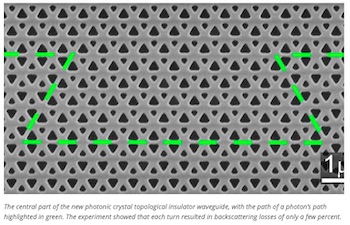
Engineers at Duke University have demonstrated a device that can direct photons of light around sharp corners with virtually no losses due to backscattering, a key property that will be needed if electronics are ever to be replaced by light-based devices.
The result was achieved with photonic crystals built on the concept of topological insulators, which won its discoverers a Nobel Prize in 2016. By carefully controlling the geometry of a crystal lattice, researchers can block light from traveling through its interior while transmitting it perfectly along its surface.
The device accomplishes its near-perfect transmittance around corners despite being much smaller than previous designs.
The Semiconductor Industry Association estimates that the number of electronic devices is increasing so rapidly that by the year 2040, there won’t be enough power in the entire world to run them all. One potential solution is to turn to massless photons to replace the electrons currently used for transmitting data. Besides saving energy, photonic systems also promise to be faster and have higher bandwidth.
Photons are already in use in some applications such as on-chip photonic communication. One drawback of the current technology, however, is that such systems cannot turn or bend light efficiently. But for photons to ever replace electrons in microchips, travelling around corners in microscopic spaces is a key.
A schematic of the new optical waveguide device showing the input and output gratings and silicon waveguide connections.
“The smaller the device the better, but of course we’re trying to minimize losses as well,” said Wiktor Walasik, a postdoctoral associate in electrical and computer engineering at Duke. “There are a lot of people working to make an all-optical computing system possible. We’re not there yet, but I think that’s the direction we’re going.”
Previous demonstrations have also shown small losses while guiding photons around corners, but the new Duke research does it on a rectangular device just 35 micrometers long and 5.5 micrometers wide—100 times smaller than previously demonstrated ring-resonator-based devices.
In the new study, which appeared online on November 12 in the journal Nature Nanotechnology, researchers fabricated topological insulators using electron beam lithography and measured the light transmittance through a series of sharp turns. Each turn only resulted in the loss of a few percent.
A closer look at the new optical waveguide device featuring a zoomed-in view of the fabricated photonic crystal topological insulator.
“Guiding light around sharp corners in conventional photonic crystals was possible before but only through a long laborious process tailored to a specific set of parameters,” said Natasha Litchinitser, professor of electrical and computer engineering at Duke. “And if you made even the tiniest mistake in its fabrication, it lost a lot of the properties you were trying to optimize.”
“But our device will work no matter its dimensions or geometry of the photons’ path and photon transport is ‘topologically protected,’” added Mikhail Shalaev, a doctoral student in Litchinitser’s laboratory and first author of the paper. “This means that even if there are minor defects in the photonic crystalline structure, the waveguide still works very well. It is not so sensitive to fabrication errors.”
The researchers point out that their device also has a large operating bandwidth, is compatible with modern semiconductor fabrication technologies, and works at wavelengths currently used in telecommunications.
Now the researchers are trying to make a waveguide that can be turned on or off at will—another important feature for all-optical photon-based technologies to ever become a reality.
This work was supported by the Army Research Office (W911NF-15-1-0152, W911NF-11-1-0297).
CITATION: “Robust Topologically Protected Transport In Photonic Crystals at Telecommunication Wavelengths,” Mikhail I. Shalaev, Wiktor Walasik, Alexander Tsukernik, Yun Xu, Natalia M. Litchinitser. Nature Nanotechnology, 12 November, 2018. DOI: 10.1038/s41565-018-0297-6
Share on:


Testimonial
"The I-Connect007 team is outstanding—kind, responsive, and a true marketing partner. Their design team created fresh, eye-catching ads, and their editorial support polished our content to let our brand shine. Thank you all! "
Sweeney Ng - CEE PCBSuggested Items
The Right Approach: Electro-Tek—A Williams Family Legacy, Part 1
10/15/2025 | Steve Williams -- Column: The Right ApproachThere is no bronze bust in the lobby or portrait in the conference room of Electro-Tek's founder—my Dad, Charles “Chuck” Williams—so with the facility closing last year after 56 years, I feel it is time to tell the story. Chuck Williams founded Electro-Tek in 1968 in our basement, eventually moving into the second floor of an old 1913 building in downtown Milwaukee that is still standing (the first of three eventual facilities).
ICT Symposium Review: Sustainability and the Circular Economy
10/09/2025 | Pete Starkey, I-Connect007It was pleasant autumnal weather as we made our way once again to Meriden, the nominal centre of England, for the 2025 Annual Symposium of the Institute of Circuit Technology. Delegates were welcomed by technical director Emma Hudson who introduced and moderated a skilfully coordinated programme, focused on the highly relevant theme of sustainability.
Hardware Engineers, Manufacturing Leaders Ready to ‘Build Better’ Electronics
10/06/2025 | Marcy LaRont, I-Connect007According to Instrumental’s dynamic CEO, Anna-Katrina Shedletsky, the Build Better Electronics Manufacturing Summit on Sept. 30 was a passion project meant to provide a forum for hardware engineering senior leadership, who have very busy jobs and limited opportunities, to share information, thought leadership, and networking opportunities. “Build Better is really about cross-pollination and sharing,” she said, as she highlighted the importance of supporting this type of sharing in tech, which may be more important than ever before.
I-Connect007 Editor’s Choice: Five Must-Reads for the Week
10/03/2025 | Andy Shaughnessy, I-Connect007It’s been a busy week. We’ve been covering PCB West, and we’ll be bringing you a variety of news and interviews from the show in the next few weeks. We’ll also be attending SMTA International later this month, and productronica as trade show season rolls on. This week, we have a number of interesting columns and news items. We start with a positive story about North American PCB sales, which were heading in the right direction in August. Don Ball writes about the ins and out of working with overseas partners, and there’s a great column by Dan Beaulieu on avoiding the temptation to offer discounts when your customer gets squirrely.
Understanding Signal Integrity, the Foundation of High-Speed Digital Design
09/25/2025 | Stephen V. Chavez, Siemens EDASignal integrity has become a critical factor in ensuring reliable performance in high-speed digital systems. As data rates continue to increase, engineers must understand the fundamental principles that govern how signals propagate through transmission lines and how to mitigate common issues that can degrade signal quality.