


 Dan’s Biz Bookshelf: 'Breakneck: China’s Quest to Engineer the Future'
 The Chemical Connection: Managing Cumulative Process Variations for Fun and Profit
 It’s Only Common Sense: Speed Is a Strategy that Wins Customers


Cutting and Pasting with Graphene
December 12, 2018 | University of LeidenEstimated reading time: 2 minutes
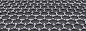
To date it has proved very difficult to convert the promises of the miracle material graphene into practical applications. Amedeo Bellunato, PhD candidate at the Leiden Institute of Chemistry, has developed a method of cutting graphene into smaller fragments using a diamond knife. He can then construct nanostructures from the fragments.
Graphene is a honeycomb structure of carbon atoms just a single atom thick. After its discovery in 2004, it seemed to be the ideal basic material for nanotechnology applications: it is super strong and it is an exceptionally good conductor of both heat and electricity. In 2013 the EU launched theGraphene Flagship a research programme with a budget of a billion euros to develop such applications as more efficient solar cells, LEDs, batteries and all kinds of sensors.
However, in his dissertation, Bellunato states that making such nanostructures is still an extremely complex production process that does not lend itself well to serial production. Also, it has proven almost impossible to selectively 'functionalize' graphene chemically, i.e. to connect other chemical elements, such as oxygen or nitrogen atoms, to the edges of a graphene nanostructure. It is important to be able to do this in order to make graphene into a versatile nanomaterial with multiple applications.
The microtome that cuts exceptionally precise strips of of graphene. The sandwich with the graphene (inset) is the transparent block to the left, the diamond knife can be seen at the edge of the blue container.
Graphene Sandwich
Inspired by earlier experiments, Bellunato decided to take a different approach, namely to take a sandwich of plastic and metal with a layer of graphene in the middle, and to literally cut it into fragments. He does this using a microtome, a diamond knife that can cut fragments with nanometre precision.
In the cutting edge of the sandwich, a perfectly clean, one-atom-thick edge of graphene is exposed, to which other atoms or molecules can be connected by chemical means. The graphene slice can also be connected to an electrical current, turning it into an electrochemical cell. This can be compared with the electrochemical coating of a metal, but then at nanoscale, since only the edge of the graphene is coated. Bellunato was also able to build a sandwich of nanopores and nanogaps of graphene using microscopically thin strips.
Kruiselings
It also proved possible to make a so-called tunnel junction. This occurs between two electrical conductors, when they are within a few nanometres of one another at a particular point. A minuscule current can then flow between the two conductors. As the flow of energy is very sensitive to the distance between the conductors, this tunnel effect forms the basis for all kinds of extremely sensitive sensors.
Bellunato: 'This tunnel junction is not new. It is a matter of refining the technique, and then it should have practical applications within five years or so.' The unconventional technique that he developed will not primarily be used in consumer products, he expects, but rather in advanced research instruments.
Text: Arnout Jaspers
Share on:


Testimonial
"Our marketing partnership with I-Connect007 is already delivering. Just a day after our press release went live, we received a direct inquiry about our updated products!"
Rachael Temple - AlltematedSuggested Items
Podcast Episode 2—AI Is Changing the Rules: Are Your PCB Materials Ready?
03/10/2026 | I-Connect007I-Connect007 announces the release of the second episode in its new six-part podcast series, PCB Materials: The Backbone and Future of Electronics. In “5G, AI & Beyond—Designing for High-Speed Performance,” we explore how artificial intelligence is reshaping the rules of electronics design, demanding unprecedented speed, power, and high-frequency performance that push beyond the limits of traditional materials. As AI applications scale rapidly, are yesterday’s materials becoming obsolete?
STMicroelectronics Completes Acquisition of NXP’s MEMS Business
02/03/2026 | STMicroelectronicsSTMicroelectronics, a global semiconductor leader serving customers across the spectrum of electronics applications, completed the acquisition of NXP Semiconductors’ (NASDAQ: NXPI) MEMS sensors business.
Real Time with... productronica 2025: Navigating Changes in the EMEA Market—Insights from Ventec Experts
12/10/2025 | Real Time with...productronicaVentec's Mark Goodwin and Pesh Patel explore the EMEA market's structural changes, including Panasonic's factory closure and its effects on laminators. They discuss the transition to low DK glass and the influence of the AI boom. Mark highlights the need for effective inventory management, while Pesh presents the glass-free revolution, showcasing new materials and resin technologies that improve performance and expand applications beyond traditional circuit boards.
Real Time with... productronica 2025: Enhancing Manufacturing With Conformal Coatings From MacDermid Alpha
12/04/2025 | Real Time with...productronicaSaskia Hogan, global product manager for conformal coatings at MacDermid Alpha Electronics Solutions, discusses the role of coatings in improving manufacturing efficiency and sustainability. She addresses challenges faced by customers, such as harsher environments and cost pressures, while emphasizing the need for high reliability in critical applications.
On the Line With… American Standard Circuits: Ultra HDI Releases Episode 10
12/03/2025 | I-Connect007I-Connect007 is pleased to announce the release of Episode 10 of On the Line With… American Standard Circuits: Ultra HDI. In this episode, host Nolan Johnson sits down with John Johnson of American Standard Circuits for a forward-looking discussion on how Ultra High Density Interconnect (UHDI) technology is reshaping some of the most demanding applications in the medical electronics space.