


 The Marketing Minute: Marketing With Layers
 The Right Approach: Electro-Tek—A Williams Family Legacy, Part 1
 It’s Only Common Sense: If You’re Not Differentiated, You’re Dead


Wireless Pacemaker for the Brain
January 2, 2019 | UC BerkeleyEstimated reading time: 4 minutes
A new neurostimulator developed by engineers at UC Berkeley can listen to and stimulate electric current in the brain at the same time, potentially delivering fine-tuned treatments to patients with diseases like epilepsy and Parkinson’s.
The device, named the WAND, works like a “pacemaker for the brain,” monitoring the brain’s electrical activity and delivering electrical stimulation if it detects something amiss.
In a proposed device, two of the new chips would be embedded in a chassis located outside the head. Each chip could monitor electrical activity from 64 electrodes located into the brain while simultaneously delivering electrical stimulation to prevent unwanted seizures or tremors. (credit: Rikky Muller, UC Berkeley)
These devices can be extremely effective at preventing debilitating tremors or seizures in patients with a variety of neurological conditions. But the electrical signatures that precede a seizure or tremor can be extremely subtle, and the frequency and strength of electrical stimulation required to prevent them is equally touchy. It can take years of small adjustments by doctors before the devices provide optimal treatment.
WAND, which stands for wireless artifact-free neuromodulation device, is both wireless and autonomous, meaning that once it learns to recognize the signs of tremor or seizure, it can adjust the stimulation parameters on its own to prevent the unwanted movements. And because it is closed-loop — meaning it can stimulate and record simultaneously — it can adjust these parameters in real-time.
“The process of finding the right therapy for a patient is extremely costly and can take years. Significant reduction in both cost and duration can potentially lead to greatly improved outcomes and accessibility,” said Rikky Muller assistant professor of electrical engineering and computer sciences at Berkeley. “We want to enable the device to figure out what is the best way to stimulate for a given patient to give the best outcomes. And you can only do that by listening and recording the neural signatures.”
WAND can record electrical activity over 128 channels, or from 128 points in the brain, compared to eight channels in other closed-loop systems. To demonstrate the device, the team used WAND to recognize and delay specific arm movements in rhesus macaques. The device is described in a study that appeared today (Dec. 31) in Nature Biomedical Engineering.
Ripples in a Pond
Simultaneously stimulating and recording electrical signals in the brain is much like trying to see small ripples in a pond while also splashing your feet — the electrical signals from the brain are overwhelmed by the large pulses of electricity delivered by the stimulation.
Currently, deep brain stimulators either stop recording while delivering the electrical stimulation, or record at a different part of the brain from where the stimulation is applied — essentially measuring the small ripples at a different point in the pond from the splashing.
“In order to deliver closed-loop stimulation-based therapies, which is a big goal for people treating Parkinson’s and epilepsy and a variety of neurological disorders, it is very important to both perform neural recordings and stimulation simultaneously, which currently no single commercial device does,” said former UC Berkeley postdoctoral associate Samantha Santacruz, who is now an assistant professor at the University of Texas in Austin.
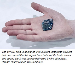
Researchers at Cortera Neurotechnologies, Inc., led by Rikky Muller, designed the WAND custom integrated circuits that can record the full signal from both the subtle brain waves and the strong electrical pulses. This chip design allows WAND to subtract the signal from the electrical pulses, resulting in a clean signal from the brain waves.
A close up picture of an integrated circuit
WAND’s custom integrated circuits. (credit: Rikky Muller, UC Berkeley)
Existing devices are tuned to record signals only from the smaller brain waves and are overwhelmed by the large stimulation pulses, making this type of signal reconstruction impossible.
“Because we can actually stimulate and record in the same brain region, we know exactly what is happening when we are providing a therapy,” Muller said.
In collaboration with the lab of electrical engineering and computer science professor Jan Rabaey, the team built a platform device with wireless and closed-loop computational capabilities that can be programmed for use in a variety of research and clinical applications.
In experiments lead by Santacruz while a postdoc at UC Berkeley, and by and electrical engineering and computer science professor Jose Carmena, subjects were taught to use a joystick to move a cursor to a specific location. After a training period, the WAND device was capable of detecting the neural signatures that arose as the subjects prepared to perform the motion, and then deliver electrical stimulation that delayed the motion.
“While delaying reaction time is something that has been demonstrated before, this is, to our knowledge, the first time that it has been demonstrated in a closed-loop system based on a neurological recording only,” Muller said.
“In the future we aim to incorporate learning into our closed-loop platform to build intelligent devices that can figure out how to best treat you, and remove the doctor from having to constantly intervene in this process,” said Muller said.
Share on:


Testimonial
"We’re proud to call I-Connect007 a trusted partner. Their innovative approach and industry insight made our podcast collaboration a success by connecting us with the right audience and delivering real results."
Julia McCaffrey - NCAB GroupSuggested Items
Elementary Mr. Watson: Chasing Checkmarks, Not Signal Integrity
10/01/2025 | John Watson -- Column: Elementary, Mr. WatsonFor the September 2025 issue of Design007 Magazine on signal integrity, I explored how the PCB is similar to a military obstacle course: walls that sap energy like impedance mismatches, barbed wire that cuts like crosstalk, and mud pits that drag a signal down like attenuation. The takeaway was clear that a PCB is not a flat drawing; it's an electromagnetic ecosystem filled with hazards that test every signal that dares to cross it. The real danger lies not in the obstacles themselves, but in the fact that many designers never see them.
Signal Integrity: A Game of Margins
09/25/2025 | Andy Shaughnessy, Design007 MagazineAs the founder of Wild River Technology, Al Neves deals with some of the most challenging aspects of signal integrity. Wild River’s engineers consult with high-tech companies that work at very high speeds and frequencies, often above 100G. Al is always a fun interview, so we asked him to share his thoughts on the current state of signal integrity engineering.
Understanding Signal Integrity, the Foundation of High-Speed Digital Design
09/25/2025 | Stephen V. Chavez, Siemens EDASignal integrity has become a critical factor in ensuring reliable performance in high-speed digital systems. As data rates continue to increase, engineers must understand the fundamental principles that govern how signals propagate through transmission lines and how to mitigate common issues that can degrade signal quality.
Beyond Design: Slaying Signal Integrity Villains
09/17/2025 | Barry Olney -- Column: Beyond DesignHigh-speed PCB design is a balancing act, where subtle oversights can develop into major signal integrity nightmares. Some culprits lie dormant during early validation, only to reveal themselves later through workflow disruptions and elusive performance bottlenecks. Take crosstalk, for example. What begins as a stray signal coupling between traces can ripple through the design, ultimately destabilizing the power distribution network. Each of these troublemakers operates with signature tactics, but they also have well-known vulnerabilities.
Staying on Top of Signal Integrity Challenges
09/16/2025 | Andy Shaughnessy, Design007 MagazineOver the years, Kris Moyer has taught a variety of advanced PCB design classes, both online IPC courses and in-person classes at California State University-Sacramento, where he earned his degrees in electrical engineering. Much of his advanced curriculum focuses on signal integrity, so we asked Kris to discuss the trends he’s seeing in signal integrity today, the SI challenges facing PCB designers, and his go-to techniques for controlling or completely eliminating SI problems.