


 It’s Only Common Sense: The Underrated Business Strategy of Joy
 Punching Out: How to Stay Focused in Business and M&A
 Marcy’s Musings: Old School vs. New School—When Does It Matter?


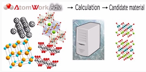
Japanese researchers have found an approach to more quickly and successfully identify superconducting materials.
"The data-driven approach shows promising power to accelerate the discovery of new thermoelectric and superconducting materials," the researchers say in their study published in the journal Science and Technology of Advanced Materials.
Superconductors are materials that conduct electricity with virtually no resistance. Superconducting materials have improved the field of magnetic resonance imaging (MRI) and have led to the development of particle colliders that can be used for research related to splitting atoms. Currently available superconducting materials can only perform at extremely low temperatures. If researchers can find superconducting materials that work at ambient temperature, electricity could be conducted over large distances without energy loss.
Current approaches to searching for these materials are somewhat random, and results strongly depend on researcher's intuition, experience and luck. Materials scientist Yoshihiko Takano of Japan's National Institute for Materials Science and colleagues have shown that sifting through an inorganic materials database using specific search parameters can provide a more systematic way to finding superconducting materials.
They searched through AtomWork, a large database for inorganic materials. In a previous study using this same approach, the team identified SnBi2Se4 (a compound of tin, bismuth, and selenium) as a potential superconductor. Experiments showed that this was indeed the case.
But SnBi2Se4 requires very low temperatures and high pressures to become superconductive. The team searched once more through the database, selecting materials that have a similar crystal structure to SnBi2Se4 but a narrower 'band gap', a property related to atomic structure that allows electrons to jump up from one energy level to another and thus partake in electrical conductivity.
Their best choice was PbBi2Te4 (formed of lead, bismuth, and tellurium). They synthesised PbBi2Te4 crystals, examined their structure, chemical composition and other properties, and found that those properties met the predictions. They exposed the crystals to high pressures and varying temperatures and found that the electrical resistance of PbBi2Te4 decreased with increasing pressure, reaching a superconductive state at 10 gigapascals, about half the pressure needed for SnBi2Se4 to become superconductive.
This work "presents a case study for the important first-step for the next-generation data-driven materials science," the team concludes.
About Science and Technology of Advanced Materials (STAM) Journal
Open access journal, STAM publishes outstanding research articles across all aspects of materials science, including functional and structural materials, theoretical analyses, and properties of materials.


