


 The Marketing Minute: Marketing With Layers
 The Right Approach: Electro-Tek—A Williams Family Legacy, Part 1
 It’s Only Common Sense: If You’re Not Differentiated, You’re Dead


Chemical Synthesis of Nanotubes
January 15, 2019 | University of TokyoEstimated reading time: 2 minutes
For the first time, researchers used benzene—a common hydrocarbon—to create a novel kind of molecular nanotube, which could lead to new nanocarbon-based semiconductor applications.
Researchers from the Department of Chemistry have been hard at work in their recently renovated lab in the University of Tokyo’s Graduate School of Science. The pristine environment and smart layout affords them ample opportunities for exciting experiments. Professor Hiroyuki Isobe and colleagues share an appreciation for “beautiful” molecular structures and created something that is not only beautiful but is also a first for chemistry.
Their phenine nanotube (pNT) is beautiful to see for its pleasing symmetry and simplicity, which is a stark contrast to its complex means of coming into being. Chemical synthesis of nanotubes is notoriously difficult and challenging, even more so if you wish to delicately control the structures in question to provide unique properties and functions.
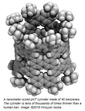
Typical carbon nanotubes are famous for their perfect graphite structures without defects, but they vary widely in length and diameter. Isobe and his team wanted a single type of nanotube, a novel form with controlled defects within its nanometer-sized cylindrical structure allowing for additional molecules to add properties and functions.
The researchers’ novel process of synthesis starts with benzene, a hexagonal ring of six carbon atoms. They use reactions to combine six of these benzenes to make a larger hexagonal ring called a cyclo-meta-phenylene (CMP). Platinum atoms are then used which allow four CMPs to form an open-ended cube. When the platinum is removed, the cube springs into a thick circle and this is furnished with bridging molecules on both ends enabling the tube shape.
It sounds complicated, but amazingly, this complex process successfully bonds the benzenes in the right way over 90 percent of the time. The key also lies in the symmetry of the molecule, which simplifies the process to assemble as many as 40 benzenes. These benzenes, also called phenines, are used as panels to form the nanometer-sized cylinder. The result is a novel nanotube structure with intentional periodic defects. Theoretical investigations show these defects imbue the nanotube with semiconductor characters.
“A crystal of pNT is also interesting: The pNT molecules are aligned and packed in a lattice rich with pores and voids,” Isobe explains. “These nanopores can encapsulate various substances which imbue the pNT crystal with properties useful in electronic applications. One molecule we successfully embedded into pNT was a large carbon molecule called fullerene (C70).”
“A team lead by Kroto/Curl/Smalley discovered fullerenes in 1985. It is said that Sir Harold Kroto fell in love with the beautiful molecule,” continues Isobe. “We feel the same way about pNT. We were shocked to see the molecular structure from crystallographic analysis. A perfect cylindrical structure with fourfold symmetry emerges from our chemical synthesis.”
“After a few decades since the discovery, this beautiful molecule, fullerene, has found various utilities and applications,” adds Isobe. “We hope that the beauty of our molecule is also pointing to unique properties and useful functions waiting to be discovered.
Share on:


Testimonial
"In a year when every marketing dollar mattered, I chose to keep I-Connect007 in our 2025 plan. Their commitment to high-quality, insightful content aligns with Koh Young’s values and helps readers navigate a changing industry. "
Brent Fischthal - Koh YoungSuggested Items
Rules of Thumb: Design007 Magazine, November 2024
11/11/2024 | I-Connect007 Editorial TeamRules of thumb are everywhere, but there may be hundreds of rules of thumb for PCB design. They’re built on design formulas, fabricators’ limitations, and tribal knowledge. And unfortunately, some longtime rules of thumb should be avoided at all costs. How do we separate the wheat from the chaff, so to speak?
Connect the Dots: Best Practices for Prototyping
09/21/2023 | Matt Stevenson -- Column: Connect the DotsPCB prototyping is a critical juncture during an electronic device’s journey from concept to reality. Regardless of a project’s complexity, the process of transforming a design into a working board is often enlightening in terms of how a design can be improved before a PCB is ready for full production.
The Drive Toward UHDI and Substrates
09/20/2023 | I-Connect007 Editorial TeamPanasonic’s Darren Hitchcock spoke with the I-Connect007 Editorial Team on the complexities of moving toward ultra HDI manufacturing. As we learn in this conversation, the number of shifting constraints relative to traditional PCB fabrication is quite large and can sometimes conflict with each other.
Asia/Pacific AI Spending Surge to Reach a Projected $78 Billion by 2027
09/19/2023 | IDCAsia/Pacific spending on Artificial Intelligence (AI) ), including software, services, and hardware for AI-centric systems will grow to $78.4 billion in 2027, according to International Data Corporation's latest Worldwide Artificial Intelligence Spending Guide.
Intel to Sell Minority Stake in IMS Nanofabrication Business to TSMC
09/13/2023 | IntelIntel Corporation announced that it has agreed to sell an approximately 10% stake in the IMS Nanofabrication business to TSMC. TSMC’s investment values IMS at approximately $4.3 billion, consistent with the valuation of the recent stake sale to Bain Capital Special Situations.