


 The Right Approach: Get Ready for ISO 9001 Version 6
 Dan’s Biz Bookshelf: ‘Still Broke: Walmart’s Remarkable Transformation'
 Driving Innovation: Depth Routing Processes—Achieving Unparalleled Precision in Complex PCBs


Atotech Presents at NEPCON Japan 2019
January 17, 2019 | AtotechEstimated reading time: 1 minute
Atotech is introducing its latest panel level plating processes and equipment solution for high resolution pattern plating during the NEPCON Japan show, held January 16 to 18, 2019, at Tokyo Big Sight.
Atotech experts are available at booth E25-16, to discuss this and other highlight products, such as their precise chemical processes and manufacturing equipment solutions, which are specifically designed to handle customers current and future needs.
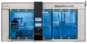
MultiPlate for FOPLP
MultiPlate is Atotech’s revolutionary plating tool which facilitates both, wafer and panel level packaging, in formats up to 650 x 610 mm. While ensuring that plating occurs at the highest current densities and achieving excellent uniformity of the plated structures, its double-sided plating capability enables improved warpage compensation. MultiPlate®’s versatility and multi-functionality helps tackle the current and future challenges for optimal performance in advanced packaging technologies.
MultiPlate Panel - Next generation plating system and Innolyte process family for panel level packaging
Other highlights include:
Novabond EX
NovaBond EX is Atotech’s new and next generation adhesion promoter for advanced package substrates. The horizontal solution provides customers with a unique and reliable process for both inner layer bonding and solder resist materials while providing a smooth interface of < 150nm Ra. The short process operates at low temperatures and short dwell times for higher productivity. NovaBond® EX is compatible with the main materials in use, or planned by, principal OEMs as defined in their future technology roadmaps.
NovaBond EX - Build-up dielectrics and solder resist materials: Excellent and stable performance after thermal stress for a wide range of ABF materials as well as the most common solder resist used in IC substrate manufacturing.
AgPrep
AgPrep is Atotech’s ultimate non-etching adhesion promoter for the lead frame industry. It substantially increases the adhesion of all commonly used molding compounds (EMC) to silver surfaces in semiconductor and LED packages. AgPrep does not create any significant changes to the original performance of the silver surface.
Visitors to the show are invited to stop by Atotech’s booth at E25-16 to learn more about these and many more new solutions for PCB, IC package and advanced packaging applications.
Share on:


Testimonial
"We’re proud to call I-Connect007 a trusted partner. Their innovative approach and industry insight made our podcast collaboration a success by connecting us with the right audience and delivering real results."
Julia McCaffrey - NCAB GroupSuggested Items
Koh Young, Fuji, and Kurtz ERSA Drive Smart Manufacturing Solutions for EV and Automotive Electronics at Kunshan, China Technical Seminar
09/11/2025 | Koh YoungKoh Young Technology, the global leader in True 3D measurement-based inspection solutions, partnered with Fuji Corporation and Kurtz ERSA to host an exclusive technical seminar for leading automotive manufacturers in East China. Held on September 4 at Fuji’s factory in Kunshan, the event gathered participants representing over 35 companies.
MacDermid Alpha Presents at SMTA New Delhi, Bangalore Chapter, on Flux–OSP Interaction
09/09/2025 | MacDermid Alpha Electronics SolutionsMacDermid Alpha contributes technical insights on OSP solderability at the Bangalore Chapter, SMTA reinforcing commitment to knowledge-sharing and industry collaboration.
Electra’s ElectraJet EMJ110 Inkjet Soldermask Now in Black & Blue at Sunrise Electronics
09/08/2025 | Electra Polymers LtdFollowing the successful deployment of Electra’s Green EMJ110 Inkjet Soldermask on KLA’s Orbotech Neos™ platform at Sunrise Electronics in Elk Grove Village, Illinois, production has now moved beyond green.
Absolute EMS: The Science of the Perfect Solder Joint
09/05/2025 | Absolute EMS, Inc.Absolute EMS, Inc., a six-time award-winning provider of fast turnaround, turnkey contract electronic manufacturing services (EMS), is drawing attention to the critical role of 3D Solder Paste Inspection (SPI) in ensuring the reliability of both FLEX and rigid printed circuit board assemblies (PCBAs).
Indium Corporation to Highlight High-Reliability Solder Solutions at SMTA Guadalajara Expo
09/04/2025 | Indium CorporationIndium Corporation, a leading materials refiner, smelter, manufacturer, and supplier to the global electronics, semiconductor, thin-film, and thermal management markets, will feature a range of innovative, high-reliability solder products for printed circuit board assembly (PCBA) at the SMTA Guadalajara Expo and Tech Forum, to be held September 17-18 in Guadalajara, Mexico.