


 The Marketing Minute: Marketing With Layers
 The Right Approach: Electro-Tek—A Williams Family Legacy, Part 1
 It’s Only Common Sense: If You’re Not Differentiated, You’re Dead


5000 Times Faster Than a Computer
January 21, 2019 | Forschungsverbund Berlin e. V.Estimated reading time: 2 minutes
The absorption of light in semiconductor crystals without inversion symmetry can generate electric currents. Researchers at the Max-Born-Institute have now generated directed currents at terahertz (THz) frequencies, much higher than the clock rates of current electronics. They show that electronic charge transfer between neighboring atoms in the crystal lattice represents the underlying mechanism.
Solar cells convert the energy of light into an electric direct current (DC) which is fed into an electric supply grid. Key steps are the separation of charges after light absorption and their transport to the contacts of the device. The electric currents are carried by negative (electrons) and positive charge carriers (holes) performing so called intraband motions in various electronic bands of the semiconductor. From a physics point of view, the following questions are essential: what is the smallest unit in a crystal which can provide a photo-induced direct current (DC)? Up to which maximum frequency can one generate such currents? Which mechanisms at the atomic scale are responsible for such charge transport?
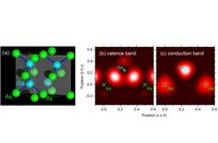
The smallest unit of a crystal is the so-called unit cell, a well-defined arrangement of atoms determined by chemical bonds. The unit cell of the prototype semiconductor GaAs is shown in Figure 1a and represents an arrangement of Ga and As atoms without a center of inversion. In the ground state of the crystal represented by the electronic valence band, the valence electrons are concentrated on the bonds between the Ga and the As atoms. Upon absorption of near-infrared or visible light, an electron is promoted from the valence band to the next higher band, the conduction band. In the new state, the electron charge is shifted towards the Ga atoms. This charge transfer corresponds to a local electric current, the interband or shift current, which is fundamentally different from the electron motions in intraband currents. Until recently, there has been a controversial debate among theoreticians whether the experimentally observed photo-induced currents are due to intraband or interband motions.
Researchers at the Max-Born-Institute in Berlin, Germany, have investigated optically induced shift currents in the semiconductor gallium arsenide (GaAs) for the first time on ultrafast time scales down to 50 femtoseconds (1 fs = 10-15 seconds). They report their results in the current issue of the journal Physical Review Letters 121, 266602 (2018) . Using ultrashort, intense light pulses from the near infrared (λ = 900 nm) to the visible (λ = 650 nm, orange color), they generated shift currents in GaAs which oscillate and, thus, emit terahertz radiation with a bandwidth up to 20 THz. The properties of these currents and the underlying electron motions are fully reflected in the emitted THz waves which are detected in amplitude and phase. The THz radiation shows that the ultrashort current bursts of rectified light contain frequencies which are 5000 times higher than the highest clock rate of modern computer technology.
The properties of the observed shift currents definitely exclude an intraband motion of electrons or holes. In contrast, model calculations based on the interband transfer of electrons in a pseudo-potential band structure reproduce the experimental results and show that a real-space transfer of electrons over the distance on the order of a bond length represents the key mechanism. This process is operative within each unit cell of the crystal, i.e., on a sub-nanometer length scale, and causes the rectification of the optical field. The effect can be exploited at even higher frequencies, offering novel interesting applications in high frequency electronics.
Share on:


Testimonial
"Our marketing partnership with I-Connect007 is already delivering. Just a day after our press release went live, we received a direct inquiry about our updated products!"
Rachael Temple - AlltematedSuggested Items
Rules of Thumb: Design007 Magazine, November 2024
11/11/2024 | I-Connect007 Editorial TeamRules of thumb are everywhere, but there may be hundreds of rules of thumb for PCB design. They’re built on design formulas, fabricators’ limitations, and tribal knowledge. And unfortunately, some longtime rules of thumb should be avoided at all costs. How do we separate the wheat from the chaff, so to speak?
Connect the Dots: Best Practices for Prototyping
09/21/2023 | Matt Stevenson -- Column: Connect the DotsPCB prototyping is a critical juncture during an electronic device’s journey from concept to reality. Regardless of a project’s complexity, the process of transforming a design into a working board is often enlightening in terms of how a design can be improved before a PCB is ready for full production.
The Drive Toward UHDI and Substrates
09/20/2023 | I-Connect007 Editorial TeamPanasonic’s Darren Hitchcock spoke with the I-Connect007 Editorial Team on the complexities of moving toward ultra HDI manufacturing. As we learn in this conversation, the number of shifting constraints relative to traditional PCB fabrication is quite large and can sometimes conflict with each other.
Asia/Pacific AI Spending Surge to Reach a Projected $78 Billion by 2027
09/19/2023 | IDCAsia/Pacific spending on Artificial Intelligence (AI) ), including software, services, and hardware for AI-centric systems will grow to $78.4 billion in 2027, according to International Data Corporation's latest Worldwide Artificial Intelligence Spending Guide.
Intel to Sell Minority Stake in IMS Nanofabrication Business to TSMC
09/13/2023 | IntelIntel Corporation announced that it has agreed to sell an approximately 10% stake in the IMS Nanofabrication business to TSMC. TSMC’s investment values IMS at approximately $4.3 billion, consistent with the valuation of the recent stake sale to Bain Capital Special Situations.