


 The Right Approach: Get Ready for ISO 9001 Version 6
 Dan’s Biz Bookshelf: ‘Still Broke: Walmart’s Remarkable Transformation'
 Driving Innovation: Depth Routing Processes—Achieving Unparalleled Precision in Complex PCBs


Atotech to Present at IPC APEX EXPO 2019
January 23, 2019 | AtotechEstimated reading time: 2 minutes
Atotech to present a new high-throw electroless Cu bath, through-hole, BMV filling, and conformal plating electrolyte, and its revolutionary direct pure EPAG final finish at the IPC APEX EXPO 2019.
BERLIN, January 23, 2019: Atotech is one of the world’s leading suppliers of specialty chemicals and equipment for the printed circuit board, package substrate and semiconductor industry. At one of the industry’s premier events, the IPC APEX Expo held at the San Diego Convention Center in San Diego, USA, from January 26 to 31, 2019, the company will exhibit and present on several new product developments.
On Tuesday, January 29, from 1:30 to 3:00 p.m., Moody Dreiza, Business Director for Electronics, North America, at Atotech USA LLC, will present “Copper Filling of Blind Microvias, Through-Holes and Cu Pillar Plating - The Present and the Future” in session S02 “PCB fabrication / Plating I”. “I will describe the reasons for development and a roadmap of dimensions for copper filled through-holes, blind microvias and other copper plated structures on PCBs by presenting aspect ratios, dimensions and results of plated through-holes used today in high volume manufacturing for blind microvia and through-hole filling with electroplated copper,” states Moody. His presentation will include feasibility studies of new electroplated structures for future applications such as copper pillar plating on IC-substrates.
On Wednesday, January 30, from 10:30 a.m. to 12:00 p.m., Roger Massey, Technical Marketing Manager at Atotech Group, will present “Developments in Electroless Copper Processes to Improve Performance in amSAP Mobile Applications” in session S13 “PCB Fabrication and Plating II”. In his presentation, Roger will highlight the benefits and robust performance of a newly developed electroless copper process for amSAP applications.
On Wednesday, January 30, from 3:30 to 4:30 p.m., Sandra Nelle, Product Manager for Surface Finishing at Atotech Group, will present “Designing a High Performance Electroless Nickel and Immersion Gold to Maximize Highest Reliability” in session S23 “PCB Surface Finishes II”. Sandra will elaborate on whether there are any ‘value added’ benefits to an HP ENIG. “I will also use data generated by Design of Experiment (DOE) to elaborate the impact of electroless nickel variables in combination with traditional and cyanide-free immersion gold on recognized quality expectations,” adds Sandra.
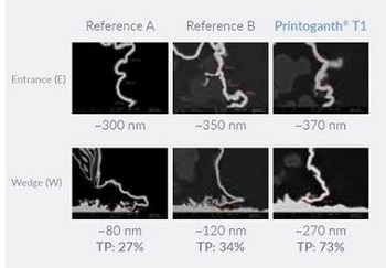
Printoganth T1 – Throwing Power Comparison
Atotech experts will also be on hand to discuss the latest chemistry and equipment at booth 311. Atotech’s latest products will be showcased at the booth, including:
- Printoganth T1, a brand new high-throw electroless copper process for advanced HDI and amSAP technology
- Inpulse 2THF, a versatile electrolyte for through-hole, blind microvia, and conformal plating for advanced HDI and substrate technology
- PallaBond, a revolutionary direct pure EPAG final finish for real fine / line applications
- Uniplate PLB Cu, a high throughput horizontal systems solution for desmear and metallization, that offers best cost, performance, and quality results in combination with Atotech’s Printoganth® T1 and Inpulse 2THF process chemistry
About Atotech
Atotech is one of the world’s leading manufacturers of specialty chemicals and equipment for the printed circuit board, IC-substrate and semiconductor industries, as well as for the decorative and functional surface finishing industries. Atotech has annual sales of $1.2 billion (2017). The company is fully committed to sustainability – we develop technologies to minimize waste and to reduce environmental impact. Atotech has its headquarters in Berlin, Germany, and employs about 4,000 people in over 40 countries.
Share on:


Testimonial
"We’re proud to call I-Connect007 a trusted partner. Their innovative approach and industry insight made our podcast collaboration a success by connecting us with the right audience and delivering real results."
Julia McCaffrey - NCAB GroupSuggested Items
Closing the Loop on PCB Etching Waste
09/09/2025 | Shawn Stone, IECAs the PCB industry continues its push toward greener, more cost-efficient operations, Sigma Engineering’s Mecer System offers a comprehensive solution to two of the industry’s most persistent pain points: etchant consumption and rinse water waste. Designed as a modular, fully automated platform, the Mecer System regenerates spent copper etchants—both alkaline and acidic—and simultaneously recycles rinse water, transforming a traditionally linear chemical process into a closed-loop system.
Driving Innovation: Depth Routing Processes—Achieving Unparalleled Precision in Complex PCBs
09/08/2025 | Kurt Palmer -- Column: Driving InnovationIn PCB manufacturing, the demand for increasingly complex and miniaturized designs continually pushes the boundaries of traditional fabrication methods, including depth routing. Success in these applications demands not only on robust machinery but also sophisticated control functions. PCB manufacturers rely on advanced machine features and process methodologies to meet their precise depth routing goals. Here, I’ll explore some crucial functions that empower manufacturers to master complex depth routing challenges.
Trouble in Your Tank: Minimizing Small-via Defects for High-reliability PCBs
08/27/2025 | Michael Carano -- Column: Trouble in Your TankTo quote the comedian Stephen Wright, “If at first you don’t succeed, then skydiving is not for you.” That can be the battle cry when you find that only small-diameter vias are exhibiting voids. Why are small holes more prone to voids than larger vias when processed through electroless copper? There are several reasons.
The Government Circuit: Navigating New Trade Headwinds and New Partnerships
08/25/2025 | Chris Mitchell -- Column: The Government CircuitAs global trade winds continue to howl, the electronics manufacturing industry finds itself at a critical juncture. After months of warnings, the U.S. Government has implemented a broad array of tariff increases, with fresh duties hitting copper-based products, semiconductors, and imports from many nations. On the positive side, tentative trade agreements with Europe, China, Japan, and other nations are providing at least some clarity and counterbalance.
How Good Design Enables Sustainable PCBs
08/21/2025 | Gerry Partida, Summit InterconnectSustainability has become a key focus for PCB companies seeking to reduce waste, conserve energy, and optimize resources. While many discussions on sustainability center around materials or energy-efficient processes, PCB design is an often overlooked factor that lies at the heart of manufacturing. Good design practices, especially those based on established IPC standards, play a central role in enabling sustainable PCB production. By ensuring designs are manufacturable and reliable, engineers can significantly reduce the environmental impact of their products.