


 The Marketing Minute: Marketing With Layers
 The Right Approach: Electro-Tek—A Williams Family Legacy, Part 1
 It’s Only Common Sense: If You’re Not Differentiated, You’re Dead


Innovative New Technique Could Pave the Way for New Generation of Flexible Electronic Components
January 30, 2019 | University of ExeterEstimated reading time: 2 minutes
Researchers at the University of Exeter have developed an innovative technique that could help create the next generation of everyday flexible electronics.
A team of engineering experts have pioneered a new way to ease production of van der Waals heterostructures with high-K dielectrics- assemblies of atomically thin two-dimensional (2-D) crystalline materials.
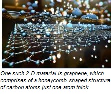
One such 2-D material is graphene, which comprises of a honeycomb-shaped structure of carbon atoms just one atom thick.
While the advantages of van der Waals heterostructures is well documented, their development has been restricted by the complicated production methods.
Now, the research team has developed a new technique that allows these structures to achieve suitable voltage scaling, improved performance and the potential for new, added functionalities by embedding a high-K oxide dielectric.
The research could pave the way for a new generation of flexible fundamental electronic components.
The research is published in the journal Science Advances.
Dr Freddie Withers, co-author of the paper and from the University of Exeter said: “Our method to embed a laser writable high-K dielectric into various van der Waals heterostructure devices without damaging the neighbouring 2D monolayer materials opens doors for future practical flexible van der Waals devices such as, field effect transistors, memories, photodetectors and LED’s which operate in the 1-2 Volt range”
The quest to develop microelectronic devices to increasingly smaller size underpins the progress of the global semiconductor industry – a collection of companies that includes the tech and communication giants Samsung and Toshiba – has been stymied by quantum mechanical effects.
This means that as the thickness of conventional insulators is reduced, the ease at which electrons can escape through the films.
In order to continue scaling devices ever smaller, researchers are looking at replacing conventional insulators with high-dielectric-constant (high-k) oxides. However, commonly used high-k oxide deposition methods are not directly compatible with 2D materials.
The latest research outlines a new method to embed a multi-functional, nanoscaled high-K oxide, only a within van der Waals devices without degrading the properties of the neighbouring 2D materials.
This new technique allows for the creation of a host of fundamental nano-electronic and opto-electronic devices including dual gated graphene transistors, and vertical light emitting and detecting tunnelling transistors.
Dr. Withers added: “The fact we start with a layered 2D semiconductor and convert it chemically to its oxide using laser irradiation allows for high quality interfaces which improve device performance.
“What’s especially interesting for me is we found this oxidation process of the parent HfS2 to take place under laser irradiation even when its sandwiched between 2 neighbouring 2D materials. This indicates that water needs to travel between the interfaces for the reaction to occur.”
Share on:


Testimonial
"Advertising in PCB007 Magazine has been a great way to showcase our bare board testers to the right audience. The I-Connect007 team makes the process smooth and professional. We’re proud to be featured in such a trusted publication."
Klaus Koziol - atgSuggested Items
Elephantech's SustainaCircuits FPC Adopted for Mass Production in OM Digital Solutions’ Interchangeable Lens
10/06/2025 | ElephantechElephantech Inc. is pleased to announce that its proprietary flexible printed circuits (FPCs) have been adopted for mass production by OM Digital Solutions Corporation in the company’s latest flagship products.
Industry Expert, Mark Finstad From Flexible Circuit Technologies Presents Ask the Flexperts at PCB West
09/22/2025 | Flexible Circuit TechnologiesFlexible Circuit Technologies., Inc/FCT is excited to announce its upcoming session, Ask the Flexperts taking place Thursday, October 2nd, from 9:00–11:00 AM at PCB West 2025. The session will be led by Mark Finstad, Director or Applications Engineering at FCT, who brings over 40 years of experience in the design, fabrication, and testing of flexible and rigid-flex circuits. Mark is an internationally recognized authority in the field, making this a must-attend event for PCB designers, engineers, and industry professionals.
Printed Electronics Market Size to Top $83.77 Billion by 2034 Driven by IoT Adoption and Flexible Device Demand
09/11/2025 | Globe NewswireThe printed electronics market size has been calculated at U$19,920 million in 2025 and is expected to grow from $23,58 million in 2026 to approximately $83,770 million by 2034.
Fresh PCB Concepts: Designing for Success at the Rigid-flex Transition Area
08/28/2025 | Team NCAB -- Column: Fresh PCB ConceptsRigid-flex PCBs come in all shapes and sizes. Manufacturers typically use fire-retardant, grade 4 (FR-4) materials in the rigid section and flexible polyimide materials in the flex region. Because of the small size, some rigid-flex PCBs, like those for hearing aid devices, are among the most challenging to manufacture. However, regardless of its size, we should not neglect the transition area between the rigid and flexible material.
Global Flexible PCB Output Expected to Surpass $20 Billion by 2025, with AI Glasses Emerging as a New Growth Driver
08/25/2025 | TPCAThe Taiwan Printed Circuit Association (TPCA) and the Industrial Technology Research Institute (ITRI) released the "2025 Global Flexible PCB Industry Outlook" in August.