


 The Marketing Minute: Marketing With Layers
 The Right Approach: Electro-Tek—A Williams Family Legacy, Part 1
 It’s Only Common Sense: If You’re Not Differentiated, You’re Dead


Semiconductor for Making Thin-Film Transistors
January 31, 2019 | Dongguk UniversityEstimated reading time: 2 minutes
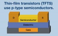
Scientists at Dongguk University have found a way to create printed p-channel thin-film transistors by using the abundantly available and environmentally friendly copper(I) iodide semiconductor at room temperature. Their energy-efficient and cost-effective fabrication method for these transistors may pave the way for developing low-cost and novel optoelectronic devices.
Transistors are the building blocks of most of the electronic devices we use every day, and research on fabricating new types of semiconducting materials for thin-film transistors (TFIs) has been ongoing for decades. Whenever new transistors or novel fabrication methods are discovered, many previously impossible applications become feasible, such as ultrahigh-definition transparent displays and flexible electronic devices. Nowadays, there is a huge demand for p-type transparent semiconductors (which are conductive due to the movement of charge carriers called “holes”) for making p-channel transistors, but when compared to the n-type counterparts, their use is limited by chemical instability and poor electric properties.
To overcome these limitations, a research team at Dongguk University led by Prof. Yong-Young Noh focused on developing a p-type transparent semiconductor for TFTs using a metal halide like copper(I) iodide (CuI), instead of metal oxide. “The naturally abundant and environment friendly constitutional elements of CuI make it more appropriate for large-scale printed transparent electronics. More importantly, CuI has a higher hole mobility than other p-type oxide-based semiconductors,” explains Prof. Noh.
However, CuI had been barely used as a semiconductor for TFTs because its hole concentration is so high that it results in uncontrollable conductivity (transistors are generally meant to be easily turned on and off at high speeds, that is, they are meant to be switchable from a conductive to a non-conductive state). Moreover, standard solution-based processing for making thin films generally requires a heat treatment called “annealing,” which is energy and time consuming.
The researchers found out that it is possible to reduce the conductivity of CuI-based thin films by making them even thinner and thus suitable for fabricating TFTs with the performance that is currently in demand for many applications. Additionally, these CuI thin films do not require annealing at all and can be processed at room temperature. This saves energy and makes them more cost-effective.
The team tested multiple processing conditions and fabricated various different TFTs to determine the origin of the enhanced device properties and to demonstrate the potential uses of CuI as a thin-film p-type semiconductor. “We believe that this work opens the floodgate for room-temperature, low-cost, printed transparent p-type transistors for diverse optoelectronic devices,” concludes Prof. Noh.
Share on:


Testimonial
"Our marketing partnership with I-Connect007 is already delivering. Just a day after our press release went live, we received a direct inquiry about our updated products!"
Rachael Temple - AlltematedSuggested Items
Episode 6 of Ultra HDI Podcast Series Explores Copper-filled Microvias in Advanced PCB Design and Fabrication
10/15/2025 | I-Connect007I-Connect007 has released Episode 6 of its acclaimed On the Line with... American Standard Circuits: Ultra High Density Interconnect (UHDI) podcast series. In this episode, “Copper Filling of Vias,” host Nolan Johnson once again welcomes John Johnson, Director of Quality and Advanced Technology at American Standard Circuits, for a deep dive into the pros and cons of copper plating microvias—from both the fabricator’s and designer’s perspectives.
Nolan’s Notes: Tariffs, Technologies, and Optimization
10/01/2025 | Nolan Johnson -- Column: Nolan's NotesLast month, SMT007 Magazine spotlighted India, and boy, did we pick a good time to do so. Tariff and trade news involving India was breaking like a storm surge. The U.S. tariffs shifted India from one of the most favorable trade agreements to the least favorable. Electronics continue to be exempt for the time being, but lest you think that we’re free and clear because we manufacture electronics, steel and aluminum are specifically called out at the 50% tariff levels.
MacDermid Alpha & Graphic PLC Lead UK’s First Horizontal Electroless Copper Installation
09/30/2025 | MacDermid Alpha & Graphic PLCMacDermid Alpha Electronics Solutions, a leading supplier of integrated materials and chemistries to the electronics industry, is proud to support Graphic PLC, a Somacis company, with the installation of the first horizontal electroless copper metallization process in the UK.
Electrodeposited Copper Foils Market to Grow by $11.7 Billion Over 2025-2032
09/18/2025 | Globe NewswireThe global electrodeposited copper foils market is poised for dynamic growth, driven by the rising adoption in advanced electronics and renewable energy storage solutions.
MacDermid Alpha Showcases Advanced Interconnect Solutions at PCIM Asia 2025
09/18/2025 | MacDermid Alpha Electronics SolutionsMacDermid Alpha Electronic Solutions, a global leader in materials for power electronics and semiconductor assembly, will showcase its latest interconnect innovations in electronic interconnect materials at PCIM Asia 2025, held from September 24 to 26 at the Shanghai New International Expo Centre, Booth N5-E30