


 The Marketing Minute: Marketing With Layers
 The Right Approach: Electro-Tek—A Williams Family Legacy, Part 1
 It’s Only Common Sense: If You’re Not Differentiated, You’re Dead


New Materials and Structures for Infrared Sensing
February 4, 2019 | ICFOEstimated reading time: 1 minute
The Optoelectronics research group led by ICREA Valerio Pruneri studies and develops new advanced materials and devices for the photonics industry as well as search to improve sensing techniques with these materials. In two studies, recently published in NanoLettes and Advanced Optical Materials, a team of ICFO researchers has been able to report on the following achievements that could improve the sensing capabilities of nanostructures based on graphene.
In the first study, ICFO researchers Kavitha K. Gopalan, Bruno Paulillo, Daniel Rodrigo, and Nestor Bareza, led by ICREA Prof. at ICFO Valerio Pruneri, in collaboration with David M.A. Mackenzie, Patrick R. Whelan, and Abhay Shivayogimath from the Technical University of Denmark, have reported, for the first time, using graphene nanostructures and a scalable nanoimprint technique to fabricate a tunable graphene nanohole array surface capable of sensing plasmonic vibrations in the mid-infrared range (∼1300–1600 cm–1). Such properties make it an interesting nanostructure for industrial applications (such as mid-infrared biosensors or photodetectors) since this technique is capable of exciting multiple plasmon modes, allowing it to do multiband sensing, something not feasible with nanoribbons or other localized resonant structures.
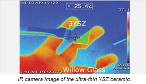
In the second study, ICFO researchers Kavitha K. Gopalan, Daniel Rodrigo, Bruno Paulillo, led by ICREA Prof at ICFO Valerio Pruneri, in collaboration with Kamal K. Soni from Corning Inc, have reported on the use of yttria‐stabilized zirconia (YSZ) ceramic as a flexible and stable platform for infrared nano-optics. In their study, the team of researchers combined the YSZ substrate with metallic nanostructures and graphene to demonstrate new plasmonic, polarizing, and transparent heating devices, overcoming the frailness and long-term functionality issues that other substrates, such as calcium fluoride and zinc selenide, present. They also showed that this material is mechanically flexible, ideally suited for making foldable or bendable devices, and for low‐cost large‐scale roll‐to‐roll fabrication processes. Such discovery proves that this material is ideal for infrared applications, which could cover thermal imaging to chemical and biological vibrational spectroscopy, among others.
Share on:


Testimonial
"In a year when every marketing dollar mattered, I chose to keep I-Connect007 in our 2025 plan. Their commitment to high-quality, insightful content aligns with Koh Young’s values and helps readers navigate a changing industry. "
Brent Fischthal - Koh YoungSuggested Items
ITW EAE Despatch Ovens Now Support ASTM 5423 Testing
10/15/2025 | ITW EAEAs the demand for high-performance electrical insulation materials continues to grow—driven by the rapid expansion of electric vehicles (EVs) and energy storage systems—thermal processing has become a critical step in material development.
Beyond Thermal Conductivity: Exploring Polymer-based TIM Strategies for High-power-density Electronics
10/13/2025 | Padmanabha Shakthivelu and Nico Bruijnis, MacDermid Alpha Electronics SolutionsAs power density and thermal loads continue to increase, effective thermal management becomes increasingly important. Rapid and efficient heat transfer from power semiconductor chip packages is essential for achieving optimal performance and ensuring long-term reliability of temperature-sensitive components. This is particularly crucial in power systems that support advanced applications such as green energy generation, electric vehicles, aerospace, and defense, along with high-speed computing for data centers and artificial intelligence (AI).
Is Glass Finally Coming of Age?
10/13/2025 | Nolan Johnson, I-Connect007Substrates, by definition, form the base of all electronic devices. Whether discussing silicon wafers for semiconductors, glass-and-epoxy materials in printed circuits, or the base of choice for interposers, all these materials function as substrates. While other substrates have come and gone, silicon and FR-4 have remained the de facto standards for the industry.
Creative Materials to Showcase Innovative Functional Inks for Medical Devices at COMPAMED 2025
10/09/2025 | Creative Materials, Inc.Creative Materials, a leading manufacturer of high-performance functional inks and coatings, is pleased to announce its participation in COMPAMED 2025, taking place November 17–20 in Düsseldorf, Germany.
Jiva Leading the Charge Toward Sustainable Innovation
09/30/2025 | Marcy LaRont, PCB007 MagazineEnvironmental sustainability in business—product circularity—is a high priority these days. “Circularity,” the term meant to replace “recycling,” in its simplest definition, describes a full circle life for electronic products and all their elements. The result is re-use or a near-complete reintroduction of the base materials back into the supply chain, leaving very little left for waste. For what cannot be reused productively, the ultimate hope is to have better, less harmful means of disposal and/or materials that can seamlessly and harmlessly decompose and integrate back into the natural environment. That is where Jiva and Soluboard come in.