


 Trouble in Your Tank: Understanding Interconnect Defects, Part 1
 It’s Only Common Sense: Marketing Isn’t Fluff, It’s Ammunition
 Driving Innovation: Mechanical and Optical Processes During Rigid-flex Production


X-Rays Reveal Why Adding a Bit of Salt Improves Perovskite Solar Cells
February 8, 2019 | University of California San DiegoEstimated reading time: 2 minutes
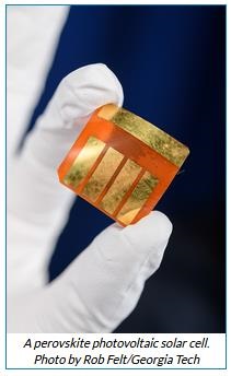
A team of researchers has reported new findings about perovskites that could pave the way to developing low-cost, high-efficiency solar cells. Using high-intensity X-ray mapping, they explain why adding small amounts of cesium and rubidium salt improves the performance of a promising class of solar cell materials, called lead-halide perovskites.
“Perovskites could really change the game in solar. They have the potential to reduce costs without giving up performance. But there’s still a lot to learn fundamentally about these materials,” said David Fenning, a professor of nanoengineering at the University of California San Diego and co-senior author of the study. “We’re looking deeper into some of the state-of-the-art chemistries to understand what drives perovskite performance and why they work so well.”
“Perovskite solar cells offer a lot of potential advantages because they are extremely lightweight and can be made with flexible plastic substrates,” said Juan-Pablo Correa-Baena, an assistant professor at the Georgia Institute of Technology who co-led the study. “To be able to compete in the marketplace with silicon-based solar cells, however, they need to be more efficient.”
In recent years, researchers have focused on testing different recipes to achieve better efficiencies, such as adding rubidium and cesium cations to lead-halide perovskites. Studies have shown that adding these alkali metal cations improves perovskite stability and performance, but little was known about why.
To answer this question, Correa-Baena teamed up with Fenning, a researcher at the UC San Diego Sustainable Power and Energy Center whose lab specializes in using X-ray imaging techniques to probe inside perovskites at the nanoscale and create high-resolution maps of their atomic structures.
“By looking at the composition within the perovskite material, we can see how each individual element plays a role in improving the performance of the device,” said Yanqi (Grace) Luo, a nanoengineering PhD student in Fenning’s Solar Energy Innovation Lab and co-first author of the study.
Their experiments revealed that adding low concentrations of either rubidium or cesium cations caused halide atoms within the material to distribute evenly, resulting in up to two percent higher conversion efficiency than perovskites without these additives.
“We found that uniformity in the chemistry and structure is what helps a perovskite solar cell operate at its fullest potential. Any heterogeneity in that backbone is like a weak link in the chain,” said Fenning.
While adding small amounts of rubidium or cesium was beneficial, the team also observed that adding too much caused some perovskite cations to cluster together, creating microscopic inactive “dead zones” in the solar cell that produce no current.
“This was surprising,” said Fenning. “Having these dead zones would typically kill a solar cell. In other materials, they act like black holes that suck in electrons from other regions and never let them go so you lose current and voltage. But in these perovskites, we saw that the dead zones around rubidium and cesium weren’t too detrimental to solar cell performance, though there was some current loss. This shows how robust these materials are but also that there’s even more opportunity for improvement.”
Ongoing studies will explore in further detail how uniform halide distribution affects the long term stability of perovskite solar cells.
Share on:


Testimonial
"The I-Connect007 team is outstanding—kind, responsive, and a true marketing partner. Their design team created fresh, eye-catching ads, and their editorial support polished our content to let our brand shine. Thank you all! "
Sweeney Ng - CEE PCBSuggested Items
Smart Eye Collaborates with Sony on Next-Generation Interior Sensing and Iris Authentication
10/09/2025 | Smart EyeSmart Eye AB, the global leader in Interior Sensing AI and Driver Monitoring Systems (DMS), announced a collaboration with Sony Semiconductor Solutions Corporation (Sony) to integrate Smart Eye’s interior sensing and biometric authentication software with Sony’s newly released IMX775 RGB-IR image sensor.
SEMICON Europa 2025 to Highlight Innovations in Advanced Packaging, Fab Management, and MEMS and Imaging Sensors to Bolster Europe’s Semiconductor Resilience
10/03/2025 | SEMISemiconductor industry experts will convene at SEMICON Europa 2025, November 18-21 at Messe München in Munich, to explore the latest trends and innovations in advanced packaging and fab management.
MEMS & Imaging Sensors Summit to Spotlight Sensing Revolution for Europe’s Leadership
09/11/2025 | SEMIIndustry experts will gather November 19-20 at the SEMI MEMS & Imaging Sensors Summit 2025 to explore the latest breakthroughs in AI-driven MEMS and imaging optimization, AR/VR technologies, and advanced sensor solutions for critical defence applications.
Direct Imaging System Market Size to Hit $4.30B by 2032, Driven by Increasing Demand for High-Precision PCB Manufacturing
09/11/2025 | Globe NewswireAccording to the SNS Insider, “The Direct Imaging System Market size was valued at $2.21 Billion in 2024 and is projected to reach $4.30 Billion by 2032, growing at a CAGR of 8.68% during 2025-2032.”
I-Connect007’s Editor’s Choice: Five Must-Reads for the Week
07/04/2025 | Marcy LaRont, I-Connect007For our industry, we have seen several bullish market announcements over the past few weeks, including one this week by IDC on the massive growth in the global server market. We’re also closely watching global trade and nearshoring. One good example of successful nearshoring is Rehm Thermal Systems, which celebrates its 10th anniversary in Mexico and the official opening of its new building in Guadalajara.