


 Driving Innovation: Mechanical and Optical Processes During Rigid-flex Production
 It’s Only Common Sense: Your Biggest Competitor Is Complacency
 The Chemical Connection: Onshoring PCB Production—Daunting but Certainly Possible


Laser Love
February 11, 2019 | Duke UniversityEstimated reading time: 4 minutes
Aditi Dighe’s eyes sparkle and she beams a megawatt smile as she remembers how she fell in love—with lasers.
She was first introduced to lasers by India’s Department of Atomic Energy, as part of a “Science Days” event at her primary school. Dighe was one of lucky handful of students who got to look behind the scenes at a research facility where scientists demonstrated some of the many uses for lasers. She saw how they were used in welding, and how they could cut beautiful, intricate patterns in different materials. To young Dighe, lasers were as close to magic as anything she had ever seen. And when she was nine years old and suffered a chlorine infection across her face that left her skin devoid of pigment, the laser treatment that she later underwent to restore her skin tone wasn’t scary. She didn’t mind the shallow furrows the lasers engraved on her skin, so entranced was she by the way the newly grafted skin pigments, activated by UV light, blossomed and spread across her face over the course of several months.
“My laser love grew stronger,” Dighe laughs. “I know that sounds silly, but it was super cool, that my skin changed colors because of the laser. It changed my life.”
As a college student, Dighe was accepted for a summer internship in the lab of Duke ECE professor Steven Cummer. Her perception of Duke ECE—small and friendly, and competitive in the field—was one part of what spurred her to apply to its PhD program after she finished her undergraduate degree in electrical engineering from the Indian Institute of Technology (IIT) Gandhinagar. The other part was the reputation of Professor Nan Jokerst, whose fascination with photonics equals Dighe’s.
Now a sixth-year PhD candidate in Jokerst’s lab, Dighe has channeled her passion into a project that could result in a patent as well as a PhD.
Dighe works on lab-on-a-chip applications, which, as their name suggests, move traditional lab processes onto the surface of a chip. Apart from their use in medical diagnostics, the devices hold potential for applications like rapid chemical analysis and environmental monitoring.
Duke ECE professor Richard Fair has been working on these devices since the early 2000s, and has learned to control microdroplets with electric currents, directing them to specific points on a silicon chip. But at that point the characteristics of the resulting configuration and constitution of droplets still must be observed using cameras, microscopes or other bulky lens setups.
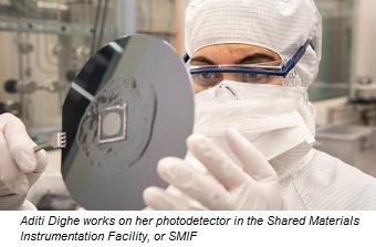
Dighe’s lab-on-a-chip design is different. A tiny fluorescence detector of her own creation is bonded to one of the two plates between which Fair’s system is sandwiched; the detector senses light emitted by fluorescent tracking particles called fluorophores in the solution, and eliminates the need for extra optical equipment for sensing.
The photodetector produces a current that corresponds with that level of intensity of light emitted by the fluorophores—high current for a high intensity light, low current for a low intensity light.
When Dighe has hammered out a predictive model for how different concentrations of solution emit different levels of light, a single measurement of current should be able to tell her the concentration of the sample she’s investigating. It takes only a tenth of a millisecond to get the necessary measurement; it’s essentially instantaneous. And in addition to saving time, the tiny scale of the lab-on-a-chip platform saves money on reagents used for testing.
The remaining challenge, said Dighe, is designing the experimental setup necessary to automate the entire process. She’s still figuring out exactly how to both direct the droplets and measure the fluorescence intensity for predictable, repeatable performance.
When she manages those tasks, Dighe said, they’ll have taken another step towards a true lab on a chip.
Dighe presented her first, long-awaited paper on her project at IEEE Sensors 2018 in Delhi in November, then followed up by presenting a poster on her work at IIT Mandi, where her mentor was delivering a keynote at the International Workshop on Nano/Micro 2D/3D Fabrication.
Jokerst, who directs the Shared Materials Instrumentation Facility (SMIF) at Duke, teaches a course on nanotechnology via a free online platform called Coursera, which has proven to be hugely popular with young people in India—an outcome that Dighe, who has done video demonstrations of a plasma-enhanced chemical vapor deposition system and electron beam evaporation for the course—finds quite gratifying.
“As a student I did not have easy access to a cleanroom,” said Dighe. “For many students who are taking introductory courses in chemical engineering or electrical engineering, to see a video like that—it’s a great learning opportunity.”
If they’re as lucky as Dighe, the simple introduction could grow into a great, career-shaping love.
Share on:


Testimonial
"Our marketing partnership with I-Connect007 is already delivering. Just a day after our press release went live, we received a direct inquiry about our updated products!"
Rachael Temple - AlltematedSuggested Items
Rules of Thumb: Design007 Magazine, November 2024
11/11/2024 | I-Connect007 Editorial TeamRules of thumb are everywhere, but there may be hundreds of rules of thumb for PCB design. They’re built on design formulas, fabricators’ limitations, and tribal knowledge. And unfortunately, some longtime rules of thumb should be avoided at all costs. How do we separate the wheat from the chaff, so to speak?
Connect the Dots: Best Practices for Prototyping
09/21/2023 | Matt Stevenson -- Column: Connect the DotsPCB prototyping is a critical juncture during an electronic device’s journey from concept to reality. Regardless of a project’s complexity, the process of transforming a design into a working board is often enlightening in terms of how a design can be improved before a PCB is ready for full production.
The Drive Toward UHDI and Substrates
09/20/2023 | I-Connect007 Editorial TeamPanasonic’s Darren Hitchcock spoke with the I-Connect007 Editorial Team on the complexities of moving toward ultra HDI manufacturing. As we learn in this conversation, the number of shifting constraints relative to traditional PCB fabrication is quite large and can sometimes conflict with each other.
Asia/Pacific AI Spending Surge to Reach a Projected $78 Billion by 2027
09/19/2023 | IDCAsia/Pacific spending on Artificial Intelligence (AI) ), including software, services, and hardware for AI-centric systems will grow to $78.4 billion in 2027, according to International Data Corporation's latest Worldwide Artificial Intelligence Spending Guide.
Intel to Sell Minority Stake in IMS Nanofabrication Business to TSMC
09/13/2023 | IntelIntel Corporation announced that it has agreed to sell an approximately 10% stake in the IMS Nanofabrication business to TSMC. TSMC’s investment values IMS at approximately $4.3 billion, consistent with the valuation of the recent stake sale to Bain Capital Special Situations.