


 Driving Innovation: Mechanical and Optical Processes During Rigid-flex Production
 It’s Only Common Sense: Your Biggest Competitor Is Complacency
 The Chemical Connection: Onshoring PCB Production—Daunting but Certainly Possible


UC Riverside Physicists Create Exotic Electron Liquid
February 12, 2019 | UC RiversideEstimated reading time: 3 minutes
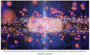
By bombarding an ultrathin semiconductor sandwich with powerful laser pulses, physicists at the University of California, Riverside, have created the first “electron liquid” at room temperature.
The achievement opens a pathway for development of the first practical and efficient devices to generate and detect light at terahertz wavelengths — between infrared light and microwaves. Such devices could be used in applications as diverse as communications in outer space, cancer detection, and scanning for concealed weapons.
The research could also enable exploration of the basic physics of matter at infinitesimally small scales and help usher in an era of quantum metamaterials, whose structures are engineered at atomic dimensions.
The UCR physicists published their findings online Feb. 4 in the journal Nature Photonics. They were led by Associate Professor of Physics Nathaniel Gabor, who directs the UCR Quantum Materials Optoelectronics Lab. Other co-authors were lab members Trevor Arp and Dennis Pleskot, and Associate Professor of Physics and Astronomy Vivek Aji.
In their experiments, the scientists constructed an ultrathin sandwich of the semiconductor molybdenum ditelluride between layers of carbon graphene. The layered structure was just slightly thicker than the width of a single DNA molecule. They then bombarded the material with superfast laser pulses, measured in quadrillionths of a second.
“Normally, with such semiconductors as silicon, laser excitation creates electrons and their positively charged holes that diffuse and drift around in the material, which is how you define a gas,” Gabor said. However, in their experiments, the researchers detected evidence of condensation into the equivalent of a liquid. Such a liquid would have properties resembling common liquids such as water, except that it would consist, not of molecules, but of electrons and holes within the semiconductor.
“We were turning up the amount of energy being dumped into the system, and we saw nothing, nothing, nothing — then suddenly we saw the formation of what we called an ‘anomalous photocurrent ring’ in the material,” Gabor said. “We realized it was a liquid because it grew like a droplet, rather than behaving like a gas.”
“What really surprised us, though, was that it happened at room temperature,” he said. “Previously, researchers who had created such electron-hole liquids had only been able to do so at temperatures colder than even in deep space.”
The electronic properties of such droplets would enable development of optoelectronic devices that operate with unprecedented efficiency in the terahertz region of the spectrum, Gabor said. Terahertz wavelengths are longer than infrared waves but shorter than microwaves, and there has existed a “terahertz gap” in the technology for utilizing such waves. Terahertz waves could be used to detect skin cancers and dental cavities because of their limited penetration and ability to resolve density differences. Similarly, the waves could be used to detect defects in products such as drug tablets and to discover weapons concealed beneath clothing.
Terahertz transmitters and receivers could also be used for faster communication systems in outer space. And, the electron-hole liquid could be the basis for quantum computers, which offer the potential to be far smaller than silicon-based circuitry now in use, Gabor said.
More generally, Gabor said, the technology used in his laboratory could be the basis for engineering “quantum metamaterials,” with atom-scale dimensions that enable precise manipulation of electrons to cause them to behave in new ways.
In further studies of the electron-hole “nanopuddles,” the scientists will explore their liquid properties such as surface tension.
“Right now, we don’t have any idea how liquidy this liquid is, and it would be important to find out,” Gabor said.
Gabor also plans to use the technology to explore basic physical phenomena. For example, cooling the electron-hole liquid to ultra-low temperatures could cause it to transform into a “quantum fluid” with exotic physical properties that could reveal new fundamental principles of matter.
In their experiments, the researchers used two key technologies. To construct the ultrathin sandwiches of molybdenum ditelluride and carbon graphene, they used a technique called “elastic stamping.” In this method, a sticky polymer film is used to pick up and stack atom-thick layers of graphene and semiconductor.
And to both pump energy into the semiconductor sandwich and image the effects, they used “multi-parameter dynamic photoresponse microscopy” developed by Gabor and Arp. In this technique, beams of ultrafast laser pulses are manipulated to scan a sample to optically map the current generated.
The research was supported by the Air Force Office of Scientific Research; the U.S. Department of Energy, Office of Science, Basic Energy Sciences; the National Science Foundation; a Cottrell Scholar Award; the Canadian Institute for Advanced Research; and NASA.
Share on:


Testimonial
"We’re proud to call I-Connect007 a trusted partner. Their innovative approach and industry insight made our podcast collaboration a success by connecting us with the right audience and delivering real results."
Julia McCaffrey - NCAB GroupSuggested Items
BAE Contract Agreed with the Republic of Türkiye for Typhoon Aircraft
10/28/2025 | BAE SystemsThe UK Government has announced a c.£5.4 billion agreement with the Republic of Türkiye for the purchase of 20 Typhoon aircraft and an associated weapons and integration package, sustaining more than 20,000 highly skilled jobs across the UK supply chain.
How PCBA Excellence Transforms High-mix Operations
09/22/2025 | Chintan Sanghani, Electronics Center for ExcellenceWith over 30 years of manufacturing excellence, our organization has built deep expertise in PCBA contract manufacturing for downhole oilfield tools. Through years of focused operational leadership in this demanding sector, we've learned that in high-mix, low-volume (HMLV) environments, traditional manufacturing approaches can create more bottlenecks than breakthroughs.
Advint Incorporated Brings Artificial Intelligence to Electroplating Training
09/11/2025 | Advint IncorporatedAdvint Incorporated is introducing a new dimension to its electroplating training programs: the integration of Artificial Intelligence (AI). This initiative reflects the company’s commitment to providing PCB fabricators and manufacturers in the USA and Canada with training that is practical, forward-looking, and directly relevant to today’s production challenges.
The Signal Integrity Issue: Design007 Magazine September 2025
09/09/2025 | I-Connect007 Editorial TeamAs the saying goes, “If you don’t have signal integrity problems now, you will eventually.” This month, our experts share a variety of design techniques that can help PCB designers and design engineers achieve signal integrity.
Semiconductors Get Magnetic Boost with New Method from UCLA Researchers
07/31/2025 | UCLA NewsroomA new method for combining magnetic elements with semiconductors — which are vital materials for computers and other electronic devices — was unveiled by a research team led by the California NanoSystems Institute at UCLA.