


 The Right Approach: Get Ready for ISO 9001 Version 6
 Dan’s Biz Bookshelf: ‘Still Broke: Walmart’s Remarkable Transformation'
 Driving Innovation: Depth Routing Processes—Achieving Unparalleled Precision in Complex PCBs


Hybrid Material May Outperform Graphene in Several Applications
March 1, 2019 | Agência FAPESPEstimated reading time: 2 minutes
Materials that are hybrid constructions (combining organic and inorganic precursors) and quasi-two-dimensional (with malleable and highly compactable molecular structures) are on the rise in several technological applications, such as the fabrication of ever-smaller optoelectronic devices.
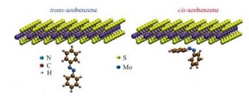
Image Caption: A structure comprising a molybdenum disulfide monolayer on an azobenzene substrate could be used to build a highly compactable and malleable quasi-two-dimensional transistor powered by light (image: atomistic representations of molybdenum disulfide monolayer with an azobenzene molecule in its trans and cis isomers/ Physical Review B)
An article published in the journal Physical Review B describes a study in this field resulting from the doctoral research of Diana Meneses Gustin and Luís Cabral, both supervised by Victor Lopez Richard, a professor at the Federal University of São Carlos (UFSCar) in Brazil. Cabral was cosupervised by Juarez Lopes Ferreira da Silva, a professor at the University of São Paulo’s São Carlos Chemistry Institute (IQSC-USP). Gustin was supported by FAPESP via a doctoral scholarship and a scholarship for a research internship abroad.
“Gustin and Cabral explain theoretically the unique optical and transport properties resulting from interaction between a molybdenum disulfide monolayer (inorganic substance MoS2) and a substrate of azobenzene (organic substance C12H10N2),” Lopez Richard told Agência FAPESP.
Illumination makes the azobenzene molecule switch isomerization and transition from a stable trans spatial configuration to a metastable cis form, producing effects on the electron cloud in the molybdenum disulfide monolayer. These effects, which are reversible, had previously been investigated experimentally by Emanuela Margapoti in postdoctoral research conducted at UFSCar and supported by FAPESP.
Gustin and Cabral developed a model to emulate the process theoretically. “They performed ab initio simulations (computational simulations using only established science) and calculations based on density functional theory (a quantum mechanical method used to investigate the dynamics of many-body systems). They also modeled the transport properties of the molybdenum disulfide monolayer when disturbed by variations in the azobenzene substrate,” Richard explained.
While the published paper does not address technological applications, the deployment of the effect to build a light-activated two-dimensional transistor is on the researchers’ horizon.
“The quasi two-dimensional structure makes molybdenum disulfide as attractive as graphene in terms of space reduction and malleability, but it has virtues that potentially make it even better. It’s a semiconductor with similar electrical conductivity properties to graphene’s and it’s more versatile optically because it emits light in the wavelength range from infrared to the visible region,” Richard said.
The hybrid molybdenum-disulfide-azobenzene structure is considered a highly promising material, but a great deal of research and development will be required if it is to be effectively deployed in useful devices.
Share on:


Testimonial
"The I-Connect007 team is outstanding—kind, responsive, and a true marketing partner. Their design team created fresh, eye-catching ads, and their editorial support polished our content to let our brand shine. Thank you all! "
Sweeney Ng - CEE PCBSuggested Items
PC Graphics Add-in Board Shipments Up 27% QoQ in 2Q25
09/03/2025 | Jon Peddie ResearchAccording to a new research report from the analyst firm Jon Peddie Research, the growth of the global PC-based graphics add-in board market reached 11.6 million units in Q2'25 and desktop PC CPUs shipments increased to 21.7 million units.
PC GPU Shipments Up 8.4% in 2Q25 on Pre-Tariff Demand
09/02/2025 | Jon Peddie ResearchJon Peddie Research reports the growth of the global PC-based graphics processor unit (GPU) market reached 74.7 million units in Q2'25, and PC CPU shipments increased to 66.9 million units.
20 Years of Center Nanoelectronic Technologies (CNT) – Backbone of German Semiconductor Research Celebrates Anniversary
08/14/2025 | Fraunhofer IPMSThe Center Nanoelectronic Technologies (CNT) of the Fraunhofer Institute for Photonic Microsystems (IPMS) is celebrating its 20th anniversary this year. Since its founding in 2005, it has developed into a pillar of applied semiconductor research in Germany and Europe. With its unique research cleanroom and equipment adhering to the 300-mm wafer industry standard, CNT is unparalleled in Germany and serves as a central innovation driver for the microelectronics industry.
Q2 Client CPU Shipments Increased 8% from Last Quarter, Up 13% YoY
08/13/2025 | Jon Peddie ResearchJon Peddie Research reports that the global client CPU market expanded for two quarters in a row, and in Q2’25, it showed unseasonal growth of 7.9% from last quarter, while server CPU shipments increased 22% year over year.
FuriosaAI Closes $125M Investment Round to Scale Production of Next-Gen AI Inference Chip
07/31/2025 | BUSINESS WIREFuriosaAI, a semiconductor company building a new foundation for AI compute, today announced it has completed a $125 million Series C bridge funding round. The investment continues a period of significant momentum for Furiosa as global demand for high-performance, efficient AI infrastructure soars.