


 Driving Innovation: Mechanical and Optical Processes During Rigid-flex Production
 It’s Only Common Sense: Your Biggest Competitor Is Complacency
 The Chemical Connection: Onshoring PCB Production—Daunting but Certainly Possible


New Optical Imaging System Could Be Deployed to Find Tiny Tumors
March 8, 2019 | MITEstimated reading time: 4 minutes
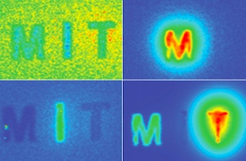
Many types of cancer could be more easily treated if they were detected at an earlier stage. MIT researchers have now developed an imaging system, named “DOLPHIN,” which could enable them to find tiny tumors, as small as a couple of hundred cells, deep within the body.
In a new study, the researchers used their imaging system, which relies on near-infrared light, to track a 0.1-millimeter fluorescent probe through the digestive tract of a living mouse. They also showed that they can detect a signal to a tissue depth of 8 centimeters, far deeper than any existing biomedical optical imaging technique.
The researchers hope to adapt their imaging technology for early diagnosis of ovarian and other cancers that are currently difficult to detect until late stages.
“We want to be able to find cancer much earlier,” says Angela Belcher, the James Mason Crafts Professor of Biological Engineering and Materials Science at MIT and a member of the Koch Institute for Integrative Cancer Research, and the newly-appointed head of MIT’s Department of Biological Engineering. “Our goal is to find tiny tumors, and do so in a noninvasive way.”
Belcher is the senior author of the study, which appears in the March 7 issue of Scientific Reports. Xiangnan Dang, a former MIT postdoc, and Neelkanth Bardhan, a Mazumdar-Shaw International Oncology Fellow, are the lead authors of the study. Other authors include research scientists Jifa Qi and Ngozi Eze, former postdoc Li Gu, postdoc Ching-Wei Lin, graduate student Swati Kataria, and Paula Hammond, the David H. Koch Professor of Engineering, head of MIT’s Department of Chemical Engineering, and a member of the Koch Institute.
Deeper Imaging
Existing methods for imaging tumors all have limitations that prevent them from being useful for early cancer diagnosis. Most have a tradeoff between resolution and depth of imaging, and none of the optical imaging techniques can image deeper than about 3 centimeters into tissue. Commonly used scans such as X-ray computed tomography (CT) and magnetic resonance imaging (MRI) can image through the whole body; however, they can’t reliably identify tumors until they reach about 1 centimeter in size.
Belcher’s lab set out to develop new optical methods for cancer imaging several years ago, when they joined the Koch Institute. They wanted to develop technology that could image very small groups of cells deep within tissue and do so without any kind of radioactive labeling.
Near-infrared light, which has wavelengths from 900 to 1700 nanometers, is well-suited to tissue imaging because light with longer wavelengths doesn’t scatter as much as when it strikes objects, which allows the light to penetrate deeper into the tissue. To take advantage of this, the researchers used an approach known as hyperspectral imaging, which enables simultaneous imaging in multiple wavelengths of light.
The researchers tested their system with a variety of near-infrared fluorescent light-emitting probes, mainly sodium yttrium fluoride nanoparticles that have rare earth elements such as erbium, holmium, or praseodymium added through a process called doping. Depending on the choice of the doping element, each of these particles emits near-infrared fluorescent light of different wavelengths.
Page 1 of 2
Share on:


Testimonial
"We’re proud to call I-Connect007 a trusted partner. Their innovative approach and industry insight made our podcast collaboration a success by connecting us with the right audience and delivering real results."
Julia McCaffrey - NCAB GroupSuggested Items
Aircraft Wire and Cable Market to surpass USD 3.2 Billion by 2034
10/30/2025 | Global Market Insights Inc.The global aircraft wire and cable market was valued at USD 1.8 billion in 2024 and is estimated to grow at a CAGR of 5.9% to reach USD 3.2 billion by 2034, according to recent report by Global Market Insights Inc.
David Schild Addresses Printed Circuit Board Issues as a Panelist at AUVSI
10/30/2025 | PCBAAOn October 28, Printed Circuit Board Association of America executive director David Schild appeared on a panel at the Association for Uncrewed Vehicle Systems International (AUVSI) conference on the topic of “First Supply Chains: Strengthening the Industrial Base for Autonomy.” PCBAA sponsored the event and Schild shared his views on issues facing the American microelectronics industry.
Real Time with... SMTAI 2025: Koh Young's Innovations in SMT Inspection Technology
10/30/2025 | Real Time with...SMTAIJoel Scutchfield discusses his background as well as Koh Young's advancements in inspection technology. The conversation covers various inspection systems, including the flagship Zenith 2 system and recent software upgrades.
BAE Contract Agreed with the Republic of Türkiye for Typhoon Aircraft
10/28/2025 | BAE SystemsThe UK Government has announced a c.£5.4 billion agreement with the Republic of Türkiye for the purchase of 20 Typhoon aircraft and an associated weapons and integration package, sustaining more than 20,000 highly skilled jobs across the UK supply chain.
Singapore’s Largest Industrial District Cooling System Begins Operations to Support STMicroelectronics’ Decarbonization Strategy
10/27/2025 | STMicroelectronicsSTMicroelectronics, a global semiconductor leader serving customers across the spectrum of electronics applications, and SP Group (SP), a leading utilities group in the Asia Pacific and Singapore’s national grid operator, have commenced operations for Singapore’s largest industrial district cooling system at STMicroelectronics’ (ST) Ang Mo Kio TechnoPark.