


 Dan’s Biz Bookshelf: ‘Abundance: How We Build a Better Future’
 Trouble in Your Tank: In Complex Systems, Design Rules Aren’t Optional
 It’s Only Common Sense: The Phone Is Still Your Competitive Advantage


Ultrathin Film Offers New Concept for Solar Energy
March 19, 2019 | University of SydneyEstimated reading time: 2 minutes
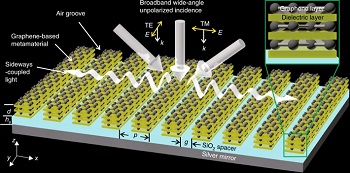
The graphene-based material is 1000 times thinner than a human hair and can be tuned for use in solar cells, solar desalination, infrared lights and optical components.
Researchers at the University of Sydney, Swinburne University of Technology and the Australian National University have collaborated to develop a solar absorbing, ultrathin film with unique properties that has great potential for use in solar thermal energy harvesting.
The 90-nanometre material is 1000 times finer than a human hair and can be rapidly heated up to 160 degrees under natural sunlight in an open environment.
This new graphene-based material also opens new avenues in:
- thermophotovoltaics (the direct conversion of heat to electricity)
- solar seawater desalination
- infrared light source and heater
- optical components: modulators and interconnects for communication devices
- photodetectors
It could even lead to the development of ‘invisible cloaking technology’ through developing large-scale thin films enclosing the objects to be ‘hidden’.
Schematic of graphene-based metamaterial absorber. Source: Nature Photonics
Professor Martijn De Sterke from the University of Sydney Nano Institute and School of Physics is Director of the Institute for Photonics and Optical Science. He said: “Through our collaboration we came up with a very innovative and successful result.
“We have developed a new class of optical material, the properties of which can be tuned for multiple uses.”
The researchers have developed a 2.5cm x 5cm working prototype to demonstrate the photo-thermal performance of the graphene-based metamaterial absorber. They have also proposed a scalable manufacture strategy to fabricate the proposed graphene-based absorber at low cost.
“This is among many graphene innovations in our group,” said Professor Baohua Jia, Research Leader, Nanophotonic Solar Technology, in Swinburne’s Centre for Micro-Photonics. “In this work, the reduced graphene oxide layer and grating structures were coated with a solution and fabricated by a laser nanofabrication method, which are both scalable and low cost.”
“Our cost-effective and scalable graphene absorber is promising for integrated, large-scale applications, such as energy-harvesting, thermal emitters, optical interconnects, photodetectors and optical modulators,” said first author of the research paper, Dr Han Lin, Senior Research Fellow at Swinburne’s Centre for Micro-Photonics.
“Fabrication on a flexible substrate and the robustness stemming from graphene make it suitable for industrial use,” Dr Keng-Te Lin, another author from Swinburne, said.
“The physical effect causing this outstanding absorption in such a thin layer is quite general and thereby opens up a lot of exciting applications,” said Dr Bjorn Sturmberg, who completed his PhD in physics at the University of Sydney in 2016 and is now a lecturer at the Australian National University.
Share on:


Subscribe
Stay ahead of the technologies shaping the future of electronics with our latest newsletter, Advanced Electronics Packaging Digest. Get expert insights on advanced packaging, materials, and system-level innovation, delivered straight to your inbox.
Subscribe now to stay informed, competitive, and connected.
Suggested Items
Sony Semiconductor Solutions, TSMC Enter Preliminary Agreement for Next-Generation Image Sensor Strategic Partnership
05/08/2026 | TSMCSony Semiconductor Solutions Corporation and TSMC announced the signing of a non-binding memorandum of understanding (MOU) to form a strategic partnership for the development and manufacturing of next-generation image sensors.
BGA Technology Expands Inspection Capabilities with Creative Electron TruView X-ray System
05/08/2026 | BGA TechnologyBGA Technology, a leading provider of advanced electronics testing and inspection services, has enhanced its inspection capabilities with the addition of a Creative Electron TruView™ Simplex X-ray system at its Holbrook, New York facility.
Molex Completes Acquisition of Teramount Ltd.
05/07/2026 | PRNewswireMolex, a global electronics leader and connectivity innovator, has completed the acquisition of Teramount Ltd., an Israel‑based developer of detachable fiber‑to‑chip connectivity solutions optimized for high‑volume Co‑Packaged Optics (CPO) and other silicon photonics applications.
IBM, Aramco Explore Collaboration to Accelerate AI and Innovation Across Saudi Arabia
05/07/2026 | IBMAramco and IBM announced their intended collaboration on opportunities to advance artificial intelligence, agentic AI, automation, material science and other mutually agreed domains in the industrial sector.
Foxconn Launches Second-Gen LEO Satellite, Begins Inter-Satellite Link Testing
05/05/2026 | FoxconnFoxconn Technology Group, the world's largest electronics manufacturing services provider, announced that its second-generation low-Earth orbit (LEO) satellites, "Pearl-1A" and "Pearl-1B," were successfully launched into their designated orbits via SpaceX's Falcon 9 rocket on the evening of May 3 (Taipei time).