It’s Only Common Sense: Stay Curious, My Friends
 The Marketing Minute: AI Is Watching Your Marketing Habits


Silver, gold and copper nanowires are leading contenders for next-generation nanoscale devices, however greater understanding of how they work and improved production methods are needed before they can be widely used, explains a recent review in the journal Science and Technology of Advanced Materials.
"Metal nanowires are used for numerous applications, but our understanding of their mechanical properties remains elusive," says Nurul Akmal Che Lah, engineer at Universiti Malaysia Pahang.
Lah and colleague Sonia Trigueros at the University of Oxford reviewed methods for synthesising and analysing silver, gold and copper nanowires for molecular-based electronics.
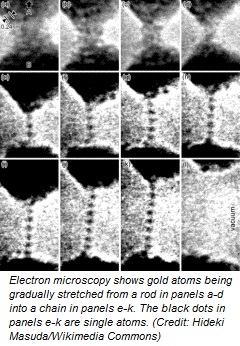
Molecular electronics uses single molecules, or nanoscale collections of molecules, to create electronic components too small to be seen with the naked eye. For example, molecular wires are one-dimensional chains of single metal atoms which conduct electric current. Molecular electronic devices can be used for a wide range of applications from storage media to catalysts and clinical treatments.
Nanomaterials have different properties from their bulk counterparts. Coinage metals in particular—silver, gold, copper and nickel—have attracted special attention because of their unique physical properties.
Recent advances in experimental techniques have allowed scientists to probe the mechanical properties of nanowires. High precision micromechanical testing devices, such as electron microscopes, scanning force microscopes and X-ray diffraction, can be used to assess crystalline structure, stress-strain relationships, atom-by-atom chemical composition, as well as electronic properties. These methods have revealed that the nanomechanical properties of nanowires are influenced by nanowire structure, surface stress and defect formation.
The researchers investigated recent developments in the synthesis and analysis of metal nanowires. Hydro-solvothermal synthesis, in which metallic structures are grown within a solution, is a relatively simple and inexpensive process. Compared with other methods that require a template or high pressures, hydro-solvothermal synthesis is best suited to industrial application as it doesn't require complex post-processing treatments.
However, synthesis methods must be improved to control the initial size, final size and morphology of the nanowires and produce high yields, whilst also being inexpensive and environmentally friendly. More work needs to be done to further optimise and improve the mechanical properties of coinage nanowires in order to harness their full potential, the researchers conclude.
Electronics at the Nanoscale
| ACN NewswireEstimated reading time: 2 minutes