


 Dan’s Biz Bookshelf: ‘Abundance: How We Build a Better Future’
 Trouble in Your Tank: In Complex Systems, Design Rules Aren’t Optional
 It’s Only Common Sense: The Phone Is Still Your Competitive Advantage


Engineering for High-Speed Devices
March 27, 2019 | University of DelawareEstimated reading time: 3 minutes
If you use a smartphone, laptop, or tablet, then you benefit from research in photonics, the study of light. At the University of Delaware, a team led by Tingyi Gu, an assistant professor of electrical and computer engineering, is developing cutting-edge technology for photonics devices that could enable faster communications between devices and thus, the people who use them.
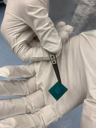
The research group recently engineered a silicon-graphene device that can transmit radiofrequency waves in less than a picosecond at a sub-terahertz bandwidth — that’s a lot of information, fast. Their work is described in a new paper published in the journal ACS Applied Electronic Materials.
“In this work, we explored the bandwidth limitation of the graphene-integrated silicon photonics for future optoelectronic applications,” said graduate student Dun Mao, the first author of the paper.
Silicon is a naturally occurring, plentiful material commonly used as a semiconductor in electronic devices. However, researchers have exhausted the potential of devices with semiconductors made of silicon only. These devices are limited by silicon’s carrier mobility, the speed at which a charge moves through the material, and indirect bandgap, which limits its ability to release and absorb light.
Now, Gu’s team is combining silicon with a material with more favorable properties, the 2D material graphene. 2D materials get their name because they are just a single layer of atoms. Compared to silicon, graphene has better carrier mobility and direct bandgap and allows for faster electron transmission and better electrical and optical properties. By combining silicon with graphene, scientists may be able to continue utilize technologies that are already used with silicon devices — they would just work faster with the silicon-graphene combination.
We’re working with? That’s what we want to figure out,” said doctoral student Thomas Kananen.
To combine silicon with graphene, the team used a method they developed and described in a paper published in 2018 in npj 2D Materials and Application. The team placed the graphene in a special place known as the p-i-n junction, an interface between the materials. By placing the graphene at the p-i-n junction, the team optimized the structure in a way that improves the responsivity and speed of the device.
This method is robust and could be easily applied by other researchers. This process takes place on a 12-inch wafer of thin material and utilizes components that are smaller than a millimeter each. Some components were made at a commercial foundry. Other work took place in UD’s Nanofabrication Facility, of which Matt Doty, associate professor of materials science and engineering, is the director.
“The UD Nanofabrication Facility (UDNF) is a staff-supported facility that enables users to fabricate devices on length scales as small as 7 nm, which is approximately 10,000 times smaller than the diameter of a human hair,” said Doty. “The UDNF, which opened in 2016, has enabled new research directions in fields ranging from optoelectronics to biomedicine to plant science.”
If you use a smartphone, laptop, or tablet, then you benefit from research in photonics, the study of light. The research involved fabricating devices at UD’s Nanofabrication Facility.
If you use a smartphone, laptop, or tablet, then you benefit from research in photonics, the study of light. The research involved fabricating devices at UD’s Nanofabrication Facility.
The combination of silicon and graphene can be used as a photodetector, which senses light and produces current, with more bandwidth and a lower response time than current offerings. All this research could add up to cheaper, faster wireless devices in the future. “It can make the network stronger, better and cheaper,” said postdoctoral associate and the first author of the npj 2D Materials and Application article Tiantian Li. “That is a key point of photonics.”
Now the team is thinking about ways to expand the applications of this material. “We’re looking at more components based on a similar structure,” said Gu.
This work is funded by grants from AFOSR and NASA, and the team has a partial collaboration with Bell Labs.
Share on:


Subscribe
Stay ahead of the technologies shaping the future of electronics with our latest newsletter, Advanced Electronics Packaging Digest. Get expert insights on advanced packaging, materials, and system-level innovation, delivered straight to your inbox.
Subscribe now to stay informed, competitive, and connected.
Suggested Items
AI Demand Drives PCB Material Market Growth
05/08/2026 | TPCAAs AI computing continues to drive a comprehensive upgrade in hardware specifications, the global printed circuit board industry is undergoing a profound structural transformation.
I-Connect007 Editor’s Choice: Five Must-Reads for the Week
05/01/2026 | Michelle Te, I-Connect007If it feels like the PCB industry is accelerating faster than ever, you’re not imagining it. From advanced materials driven by AI applications to renewed investment in domestic manufacturing—and the next generation stepping into critical roles—there’s a lot shifting at once. My selections for this week highlight where the pressure points are forming, and where the opportunities are emerging.
Electronics Manufacturing Needs Your Voice: Global Sentiment Survey Now Live
04/30/2026 | Global Electronics AssociationThe latest monthly Global Sentiment Survey from the Global Electronics Association is now open. At a time when demand uncertainty, policy shifts, energy costs, and supply chain recalibration are pulling the industry in multiple directions, the survey captures something macroeconomic data often misses: how manufacturers are actually experiencing conditions on the ground.
From Backbone to Breakthroughs: I-Connect007 Wraps PCB Materials Series with Focus on Innovation
05/06/2026 | I-Connect007I-Connect007 wraps up its six-part podcast series, PCB Materials: The Backbone and Future of Electronics, with Episode 6 and a discussion focusing on innovation. In Episode 6, Marcy LaRont speaks with Isola CTO Kirk Thompson about a critical turning point for the PCB industry as innovation accelerates. As data rates climb and demands from AI infrastructure, power density, flexible electronics, photonics, and chiplet integration intensify, traditional material assumptions are no longer sufficient.
Jiva Soluboard Getting the Attention It Deserves
04/30/2026 | Marcy LaRont, I-Connect007 MagazineJiva is a newer company that bridges the divide between PCB fabrication and product circularity or sustainability. Jiva Soluboard is the first fully recyclable laminate material ever created for PCB fabrication, and it's not going unnoticed. Stephen Driver, CEO of Jiva, gave us an update at APEX EXPO, including an exciting certification achievement in February.