


 Dan’s Biz Bookshelf: ‘Abundance: How We Build a Better Future’
 Trouble in Your Tank: In Complex Systems, Design Rules Aren’t Optional
 It’s Only Common Sense: The Phone Is Still Your Competitive Advantage


Tiny Optical Elements Could One Day Replace Traditional Refractive Lenses
March 29, 2019 | Northwestern UniversityEstimated reading time: 2 minutes
A Northwestern University research team has developed tiny optical elements from metal nanoparticles and a polymer that one day could replace traditional refractive lenses to realize portable imaging systems and optoelectronic devices.
The flat and versatile lens, a type of metalens, has a thickness 100 times smaller than the width of a human hair.
“This miniaturization and integration with detectors offers promise for high-resolution imaging in devices from small wide-angle cameras to miniature endoscopes,” said Teri W. Odom, who led the research. She is the Charles E. and Emma H. Morrison Professor of Chemistry in the Weinberg College of Arts and Sciences and chair of the department of chemistry.
The properties of metalenses depend on the rationally designed arrangement of nanoscale units. Metalenses have emerged as an attractive option for flat lenses but are currently limited by their static, as-fabricated properties and their complex and expensive fabrication.
For imaging operations such as zooming and focusing, however, most metalenses cannot adjust their focal spots without physical motion. One major reason, Odom said, is that the building blocks of these lenses are made of hard materials that cannot change shape once fabricated. It is difficult in any materials systems to adjust nanoscale-sized features on demand to obtain tunable focusing in metalenses.
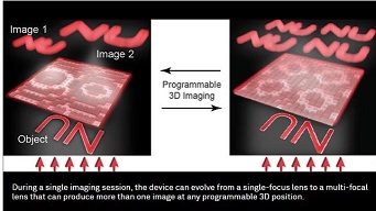
“In this study, we demonstrated a versatile imaging platform based on fully reconfigurable metalenses made from silver nanoparticles,” said Odom, a member of Northwestern’s International Institute for Nanotechnology. “During a single imaging session, our metalens device can evolve from a single-focus lens to a multi-focal lens that can form more than one image at any programmable 3D position.”
The paper, titled “Lattice-Resonance Metalenses for Fully Reconfigurable Imaging,” was published recently by the journal ACS Nano.
The Northwestern team built their lenses out of an array of cylindrical silver nanoparticles and a layer of polymer patterned into blocks on top of the metal array. By simply controlling the arrangement of the polymer patterns, the nanoparticle array could direct visible light to any targeted focal points without needing to change the nanoparticle structures.
This scalable method enables different lens structures to be made in one step of erasing and writing, with no noticeable degradation in nanoscale features after multiple erase-and-write cycles. The technique that can reshape any pre-formed polymer pattern into any desirable pattern using soft masks made from elastomers.
Share on:


Subscribe
Stay ahead of the technologies shaping the future of electronics with our latest newsletter, Advanced Electronics Packaging Digest. Get expert insights on advanced packaging, materials, and system-level innovation, delivered straight to your inbox.
Subscribe now to stay informed, competitive, and connected.
Suggested Items
Gregoire Outters Promoted to President of Teledyne Marine Group
04/06/2026 | TeledyneTeledyne Technologies Incorporated announced the promotion of Gregoire Outters to President of its Teledyne Marine Group.
Teledyne Strengthens Commitment to the Space Sector
04/01/2026 | BUSINESS WIRETeledyne Technologies Incorporated is excited to announce the integration of the company’s extensive portfolio of space-focused technologies and businesses, reinforcing its long-term commitment to the global space sector.
Teledyne to Supply Detectors for Lazuli Space Observatory
03/30/2026 | BUSINESS WIRETeledyne Space Imaging, part of Teledyne Technologies Incorporated has been awarded a contract by Schmidt Sciences to deliver advanced near-infrared (NIR) H4RG-10 flight focal plane arrays (FPAs) and custom electronics for integration into the Integral Field Spectrograph on the groundbreaking Lazuli Space Observatory.
New Superconducting Chip Could Enable Breakthrough Nondestructive Terahertz Imaging
03/23/2026 | University of GlasgowA tiny crystal chip which uses terahertz radiation to see clearly through a wide range of materials could find applications in healthcare, biological research, and security screening.
The Test Connection Adds Creative Electron Prime TruVision™ X-ray and CT System for Deeper Failure Analysis
03/05/2026 | TTCIThe Test Connection Inc. (TTCI), a trusted provider of electronic test and manufacturing solutions for more than 45 years, has added the Prime TruVision™ X-ray and computed tomography (CT) inspection system from Creative Electron to its engineering and analysis services.