


 Dan’s Biz Bookshelf: ‘Abundance: How We Build a Better Future’
 Trouble in Your Tank: In Complex Systems, Design Rules Aren’t Optional
 It’s Only Common Sense: The Phone Is Still Your Competitive Advantage


PV Nano Cell Shares Insights Following Best Ever Exhibition at LOPEC 2019
April 3, 2019 | Globe NewswireEstimated reading time: 2 minutes
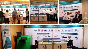
PV Nano Cell, Ltd. has announced its successful exhibition at LOPEC 2019, the leading event for Printed Electronics in Europe.
PV Nano Cell launched at the exhibition its complete solution offering for printed electronics, mass-production applications. The solution includes 3 critical components: inks, printers and printing process. The company's booth was visited by hundreds of prospects and significant leads were generated.
PV Nano Cell’s Chief of Business Development, Hanan Markovich, commented: “The exhibition was the best ever for us with an increase of 44% in total qualified registered leads compared to those registered last year. An Overwhelming 87% of the visitors to our booth work at industry-related companies whereas the rest work at research institutes and academia-related companies. More than a third of the visitors expressed high interest in mass-production applications. Furthermore, nearly half of all enquiries were made regarding a complete solution involving the ink, printer and printing process. This proves customers require a complete solution that addresses all aspects of conductive printing. Finally, the markets most discussed with us were: Automotive, PCB and Sensors. The interest in these markets demonstrates the promising, mass-production direction the industry is heading towards."
PV Nano Cell also presented its new and unique ink development for LIFT (Laser Induced Forward Transfer). The ink received significant attention from visitors and will be incorporated in the new catalog by Sigma-Aldrich. During the exhibition PV Nano Cell also demonstrated its integrated printer for design, prototyping and R&D – DemonJet.
As part of its solution strategy, the Company not only offers inks and printers but also develops the printing process for the customer. The printing process relates to the recipe, fine details and know-how of using the printer and ink to obtain the desired results for mass-production, 24/7 printing. Such know-how may include: ink properties' tweaking, printer parameters setup, printer modifications, tailored sintering instructions and more.
“This exhibition has boosted our potential customer base, especially for high volume ink consumption commercial applications and for our DemonJet™ printer. We hope the efforts we will invest in these leads in the coming months will be reflected as a rapid increase of our revenues, keeping the pace with last year’s growth,” commented Dr. Fernando de la Vega, PV Nano Cell CEO.
About PV Nano Cell, Ltd.
PV Nano Cell has developed innovative conductive inks for use in printed electronics (PE) and solar photovoltaics (PV) applications. PV Nano Cell's Sicrys™ ink family is a single-crystal, nano metric metal conductive ink delivering enhanced performance. Sicrys™ is available in silver and copper-based form, both compatible with many inkjet print heads and mass production enablers (high throughput printing, high quality and competitive pricing). Sicrys™ conductive inks are used all over the world in a range of inkjet printing applications, including photovoltaics, printed circuit boards, antennas, sensors, touchscreens and other applications.
Share on:


Subscribe
Stay ahead of the technologies shaping the future of electronics with our latest newsletter, Advanced Electronics Packaging Digest. Get expert insights on advanced packaging, materials, and system-level innovation, delivered straight to your inbox.
Subscribe now to stay informed, competitive, and connected.
Suggested Items
Driving Innovation: Selecting the Right Laser Source
04/28/2026 | Simon Khesin -- Column: Driving InnovationWhen I first joined Schmoll Maschinen, I brought experience from almost every PCB process, except for laser. As I immersed myself in laser processing, I realized why it can seem so daunting to a newcomer. The complexity arises from three intersecting factors: A vast variety of laser sources: CO2, UV-nano, green-pico, UV-pico, IR-pico, and others; a diverse range of applications: Drilling, cutting, ablation, and more; and an extensive list of materials: These have vastly different absorption rates. Choosing the right machine or laser source is rarely trivial. Even for experienced engineers, answering "Which source is best?" requires examining the business's specific goals.
Institute of Circuit Technology Spring Seminar 2026: A Bright Future in Europe
04/23/2026 | Pete Starkey, I-Connect007Through the leafy lanes and spring flowers of Warwickshire and back to Meridan, the traditional centre of England, and now officially part of the Metropolitan Borough of Solihull in the county of the West Midlands, I attended the Annual General Meeting and Spring Seminar of the Institute of Circuit Technology (ICT) on April 14. Out of the AGM came notable changes in leadership at the top of the Institute: the retirement of Mat Beadel as chair and Emma Hudson as technical director. Effective May 1, Steve Driver is the new chair, and Alun Morgan is the new technical director.
ACCM Unveils Negative and Near-zero CTE Materials for Large-Format AI Chips
04/21/2026 | Advanced Chip and Circuit MaterialsAdvanced Chip and Circuit Materials, Inc. (ACCM) has launched two new materials: Celeritas HM50, with a negative coefficient of thermal expansion (CTE) of -8 ppm/°C to offset the positive CTE and expansion of copper with temperature on circuit boards, and Celeritas HM001, with near-zero CTE and the low-loss performance needed for high-speed signal layers to 224 Gb/s and faster in artificial intelligence (AI) circuits.
Fresh PCB Concepts: Designing PCBs for Harsh Environments—Reliability Is Engineered Upstream
04/23/2026 | Team NCAB -- Column: Fresh PCB ConceptsWhen engineers hear the phrase “harsh environment,” they usually think of the extreme temperature swings, vibration and shock, pressure changes, or radiation in aerospace. However, aerospace is not the only harsh environment where electronic assemblies must survive. Automotive power electronics, downhole oil and gas tools, marine controls, rail systems, defense platforms, and industrial automation equipment all expose PCBs to environments that are equally unforgiving. The stress mechanisms may differ, but the physics does not.
Advanced Packaging for AI: Reliability Starts at the Cu/Cu/Cu Microvia Junction
04/20/2026 | Kuldip Johal, MKS' AtotechThe rapid growth of AI computing, from training clusters to inference at scale, is reshaping demand across the entire electronics supply chain. Advances in technology requirements, such as higher bandwidth, lower latency, and greater compute density, are driving the development of advanced packaging technologies and transforming the PCB industry across design, manufacturing, testing, and even architecture.