


 Dan’s Biz Bookshelf: ‘Abundance: How We Build a Better Future’
 Trouble in Your Tank: In Complex Systems, Design Rules Aren’t Optional
 It’s Only Common Sense: The Phone Is Still Your Competitive Advantage


Copper-Based Alternative for Next-Generation Electronics
April 3, 2019 | Tohoku UniversityEstimated reading time: 2 minutes
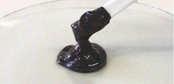
Japanese scientists have developed a technique to transform a copper-based substance into a material that mimics properties of precious and pricey metals, such as gold and silver. The new medium, made of copper nanoparticles (very small copper-based structures) has promising applications in the production of electronic devices that would otherwise depend on expensive gold and silver counterparts. It is also suitable in the fabrication of electronic components using printing technologies that are recognized as environmentally friendly production methods.
The development of the Internet of Things (IoT) has quickly increased the demand for thin and wearable electronic devices. For example, IoT depends on communication between devices, which requires antennas that have so far required expensive gold and silver-based metal composites.
To date, existing techniques for the preparation of copper nanoparticles have not been ideal as they resulted in impurities attaching to the material. Since these impurities could only be removed via extremely high temperatures, copper nanoparticles that were created at room temperature were impure and thus could not solidify into usable parts. Until now, this has been one of the hurdles to creating a more cost-effective alternative to gold and silver parts in electronic devices.The joint study between researchers at Tohoku University and Mitsui Mining & Smelting Co., Ltd in Tokyo reports the successful synthesis of copper nanoparticles with the ability of solidifying at much lower temperatures while remaining pure. The team has altered the structure of the copper nanoparticles and rendered them more stable so that they do not degrade at low temperatures.
"Copper has been an attractive alternative material in the preparation of electric circuits. The most important part of using copper is altering it so that it solidifies at low temperatures. So far, that has been difficult because copper readily interacts with the moisture in the air and degrades, which turns into unstable nanoparticles. With the methods used in this study that alter the structure of the carbon and thereby making it more stable, we have successfully overcome this instability issue," adds Kiyoshi Kanie, Ph.D., associate professor at the Institute of Multidisciplinary Research for Advanced Materials of Tohoku University.
The researchers hope to expand the application of their copper-based nanoparticles beyond just electronics. They believe that this material will be useful in other sectors as well. "Our method effectively created copper nanoparticle-based materials that can be utilized in various types of on-demand flexible and wearable devices that can be fabricated easily via printing processes at a very low cost," Kanie adds.
Share on:


Subscribe
Stay ahead of the technologies shaping the future of electronics with our latest newsletter, Advanced Electronics Packaging Digest. Get expert insights on advanced packaging, materials, and system-level innovation, delivered straight to your inbox.
Subscribe now to stay informed, competitive, and connected.
Suggested Items
Driving Innovation: Selecting the Right Laser Source
04/28/2026 | Simon Khesin -- Column: Driving InnovationWhen I first joined Schmoll Maschinen, I brought experience from almost every PCB process, except for laser. As I immersed myself in laser processing, I realized why it can seem so daunting to a newcomer. The complexity arises from three intersecting factors: A vast variety of laser sources: CO2, UV-nano, green-pico, UV-pico, IR-pico, and others; a diverse range of applications: Drilling, cutting, ablation, and more; and an extensive list of materials: These have vastly different absorption rates. Choosing the right machine or laser source is rarely trivial. Even for experienced engineers, answering "Which source is best?" requires examining the business's specific goals.
Institute of Circuit Technology Spring Seminar 2026: A Bright Future in Europe
04/23/2026 | Pete Starkey, I-Connect007Through the leafy lanes and spring flowers of Warwickshire and back to Meridan, the traditional centre of England, and now officially part of the Metropolitan Borough of Solihull in the county of the West Midlands, I attended the Annual General Meeting and Spring Seminar of the Institute of Circuit Technology (ICT) on April 14. Out of the AGM came notable changes in leadership at the top of the Institute: the retirement of Mat Beadel as chair and Emma Hudson as technical director. Effective May 1, Steve Driver is the new chair, and Alun Morgan is the new technical director.
ACCM Unveils Negative and Near-zero CTE Materials for Large-Format AI Chips
04/21/2026 | Advanced Chip and Circuit MaterialsAdvanced Chip and Circuit Materials, Inc. (ACCM) has launched two new materials: Celeritas HM50, with a negative coefficient of thermal expansion (CTE) of -8 ppm/°C to offset the positive CTE and expansion of copper with temperature on circuit boards, and Celeritas HM001, with near-zero CTE and the low-loss performance needed for high-speed signal layers to 224 Gb/s and faster in artificial intelligence (AI) circuits.
Fresh PCB Concepts: Designing PCBs for Harsh Environments—Reliability Is Engineered Upstream
04/23/2026 | Team NCAB -- Column: Fresh PCB ConceptsWhen engineers hear the phrase “harsh environment,” they usually think of the extreme temperature swings, vibration and shock, pressure changes, or radiation in aerospace. However, aerospace is not the only harsh environment where electronic assemblies must survive. Automotive power electronics, downhole oil and gas tools, marine controls, rail systems, defense platforms, and industrial automation equipment all expose PCBs to environments that are equally unforgiving. The stress mechanisms may differ, but the physics does not.
Advanced Packaging for AI: Reliability Starts at the Cu/Cu/Cu Microvia Junction
04/20/2026 | Kuldip Johal, MKS' AtotechThe rapid growth of AI computing, from training clusters to inference at scale, is reshaping demand across the entire electronics supply chain. Advances in technology requirements, such as higher bandwidth, lower latency, and greater compute density, are driving the development of advanced packaging technologies and transforming the PCB industry across design, manufacturing, testing, and even architecture.