


 Dan’s Biz Bookshelf: ‘Abundance: How We Build a Better Future’
 Trouble in Your Tank: In Complex Systems, Design Rules Aren’t Optional
 It’s Only Common Sense: The Phone Is Still Your Competitive Advantage


Golden Path Towards New Two-Dimensional Semiconductors
April 11, 2019 | Michigan Technological UniversityEstimated reading time: 3 minutes
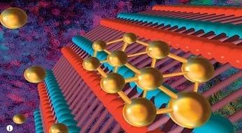
Two-dimensional (2D) semiconductors are promising for quantum computing and future electronics. Now, researchers can convert metallic gold into a semiconductor and customize the material atom-by-atom on boron nitride nanotubes.
Gold is a conductive material already widely used as interconnects in electronic devices. As electronics have gotten smaller and more powerful, the semiconducting materials involved have also shrunk. However, computers have gotten about as small as they can with existing designs — to break the barrier, researchers dive into the physics underlying quantum computing and the unusual behaviors of gold in quantum mechanics.
Researchers can convert gold into semiconducting quantum dots made of a single layer of atoms. Their energy gap, or bandgap, is formed by the quantum confinement — a quantum effect when materials behave like atoms as their sizes get so small approaching the molecular scale. These 2D gold quantum dots can be used for electronics with a bandgap that is tunable atom-by-atom.
Making the dots with monolayer of atoms is tricky and the bigger challenge is customizing their properties. When laid out on boron nitride nanotubes, researchers from Michigan Technological University have found that they can get gold quantum dots to do the near-impossible. The mechanisms behind getting gold dots to clump atom-by-atom is the focus of their new paper, recently published in ACS Nano
Energy Selective Deposition
Yoke Khin Yap, professor of physics at Michigan Tech, led the study. He explains that the behavior his team observed — atomic-level manipulation of gold quantum dots — can be seen with a scanning transmission electron microscope (STEM). The STEM’s high-powered beam of electrons enables researchers like Yap to watch atomic movement in real-time and the view reveals how gold atoms interact with the surface of boron nitride nanotubes. Basically, the gold atoms glide along the surface of the nanotubes and, they stabilize in a hover just above the hexagon honeycomb of the boron nitride nanotubes.
The atomic skiing and stopping is related to the so-called energy selective deposition. In the lab, the team takes an array of boron nitride nanotubes and runs a gold-laden mist past it; the gold atoms in the mist either stick as multilayered nanoparticles or bounce off the nanotube, but some of the more energetic ones glide along the circumference of the nanotube and stabilize, then start to clump into monolayers of gold quantum dots. The team shows that gold preferentially deposits behind other gold particles that have stabilized.
“The surface of boron nitride nanotubes are atomically smooth, there are no defects on the surface, it’s a neatly arranged honeycomb,” Yap said, adding that the nanotubes are chemically inert and there is no physical bond between the nanotubes and gold atoms. “It’s much like skiing: You can’t ski on a bumpy and sticky hill with no snow, ideal conditions make it much better. The smooth surface of the nanotubes is like fresh powder.”
Dream Nanotechnology
The search for new materials for future electronics and quantum computing has led researchers down many paths. Yap hopes that by demonstrating the effectiveness of gold, other researchers will be inspired to pay attention to other metal monolayers at the molecular-scale.
“This is a dream nanotechnology,” Yap said. “It is a molecular-scale technology tunable by atom with an ideal bandgap in the visible light spectra. There is a lot of promise in electronic and optical devices.”
The team’s next steps include further characterization and incorporating device fabrication to demonstrate all-metal electronics. Potentially, monolayers of metal atoms could make up the entirety of future electronics, which will save a lot of manufacturing energy and materials.
This work was performed in collaboration Ravindra Pandey, professor of physics at Michigan tech, whose team contributed the theoretical model, and Juan-Carlos Idrobo, scientist at the Center for Nanophase Materials Sciences at Oak Ridge National Laboratory.
About Michigan Technological University
Michigan Technological University is a public research university, home to more than 7,000 students from 54 countries. Founded in 1885, the University offers more than 120 undergraduate and graduate degree programs in science and technology, engineering, forestry, business and economics, health professions, humanities, mathematics, and social sciences. Our campus in Michigan’s Upper Peninsula overlooks the Keweenaw Waterway and is just a few miles from Lake Superior.
Share on:


Subscribe
Stay ahead of the technologies shaping the future of electronics with our latest newsletter, Advanced Electronics Packaging Digest. Get expert insights on advanced packaging, materials, and system-level innovation, delivered straight to your inbox.
Subscribe now to stay informed, competitive, and connected.
Suggested Items
I-Connect007 Editor’s Choice: Five Must-Reads for the Week
05/08/2026 | Marcy LaRont, I-Connect007This week, I’ve selected some outstanding interviews that you’ll want to take note of. First, is a roundtable discussion featuring three dynamic industry cybersecurity experts. Please watch this important discussion that affects us all. Following that, I spotlight the IPC-2581 Consortium, which explains why IPC-2581 is the standard to replace Gerber data for manufacturing. Next, I am including my interview with PCBAA and AAM, who collaborated to release a short documentary on U.S. PCB manufacturing.
Global Electronics Association to Testify at the Office of the U.S. Trade Representative Panel on Section 301 Structural Excess Capacity
05/08/2026 | Global Electronics AssociationChris Mitchell, Vice President for Global Government Relations at the Global Electronics Association, will testify before the Office of the U.S. Trade Representative (USTR) Panel on Section 301 Structural Excess Capacity on Friday, May 8.
Kimball Electronics Reports Q3 Results With Double-Digit Sequential Medical Sales Growth
05/07/2026 | Kimball ElectronicsKimball Electronics, Inc. announced financial results for the third quarter ended March 31, 2026.
Hall of Fame Spotlight Series: Highlighting Karen McConnell
05/07/2026 | Dan Feinberg, I-Connect007In 2021, Karen McConnell was awarded the Raymond E. Pritchard Hall of Fame award in recognition of her contributions to the Association and the electronics industry. As a senior staff member and CAD/CAM engineer at Northrop Grumman Enterprise Services, her primary responsibility was to develop a common, shared EDM (Electronic Document Management) library to support the electrical and PCB design tool initiatives across Northrop Grumman Mission Systems.
IMI Reports Stronger Performance and Return to Profitability in 2025
05/06/2026 | IMIIntegrated Microelectronics, Inc. (IMI) reported a significantly improved performance in 2025, reflecting the positive results of its multi year transformation focused on operational efficiency, portfolio optimization, and strengthening core capabilities.