


 The Chemical Connection: Onshoring PCB Production—Daunting but Certainly Possible
 It’s Only Common Sense: The Phone Is Still Mightier Than the Keyboard


New Tunable Nanomaterials Possible via Flexible Process
April 11, 2019 | University of BathEstimated reading time: 2 minutes
Physicists at the University of Bath have developed a flexible process allowing the synthesis in a single flow of a wide range of novel nanomaterials with various morphologies, with potential applications in areas including optics and sensors.
The nanomaterials are formed from Tungsten Disulphide – a Transition Metal Dichalcogenide (TMD)—and can be grown on insulating planar substrates without requiring a catalyst. TMDs are layered materials, and in their two-dimensional form can be considered the inorganic analogues of graphene.
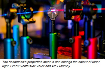
The various Tungsten Disulphide morphologies synthesized—two-dimensional sheets growing parallel to the substrate, nanotubes, or a nanomesh resembling a ‘field of blades’ growing outwards from the substrate—are possible due to Dr. Zichen Liu’s PhD research at Bath to split the growth process into two distinct stages. Through this decoupling, the growth process could be routed differently than in more conventional approaches, and be guided to produce all these material morphologies.
So far, the ‘field of blades’ morphology has shown powerful optical properties, including strong non-linear effects such as Second Harmonic Generation, that is, doubling the frequency and halving the wavelength of laser light, changing its colour as it does so. The strength of these effects opens up a range of optical applications for the material.
Dr Adelina Ilie, from the University of Bath’s Department of Physics, who led the research, said: “The simplicity of this process is important from the standpoint that it allows us to obtain practically all phases of this Transition Metal Dichalcogenide, from in-plane to out-of-plane, as well as from two-dimensional sheets to one-dimensional nanotubes and everything between. Usually different processes are used to create two-dimensional or one-dimensional morphologies. Our process, instead, leads to tunable materials with tunable properties.
“The ‘field of blades’ morphology is entirely new, and due to its very large effective surface area, might be of interest not only for the non-linear optical properties we showed so far, but also for application in various sensing technologies. We are exploring all these avenues now.”
Professor Ventsislav Valev, who tested the nanomesh for optical properties added: “We haven’t actually been able to test the upper limits of the optical effects yet because the signal is too strong for the equipment we used to probe it. We are talking about a material that is one or two atoms in thickness; it is quite extraordinary. Its arrangement into a ‘field of blades’ clearly increases the signal.”
The team plans to continue to explore the properties of the materials.
The research was supported by the University of Bath, the Engineering and Physical Sciences Research Council, and the Royal Society.
Share on:


Testimonial
"Your magazines are a great platform for people to exchange knowledge. Thank you for the work that you do."
Simon Khesin - Schmoll MaschinenSuggested Items
The Marketing Minute: Marketing With Layers
10/15/2025 | Brittany Martin -- Column: The Marketing MinuteMarketing to a technical audience is like crafting a multilayer board: Each layer serves a purpose, from the surface story to the buried detail that keeps everything connected. At I-Connect007, we’ve learned that the best marketing campaigns aren’t built linearly; they’re layered. A campaign might start with a highly technical resource, such as an in-depth article, a white paper, or a podcast featuring an engineer delving into the details of a process. That’s the foundation, the substance that earns credibility.
Taking Control of PCB Verification One Step at a Time
10/09/2025 | Kirk Fabbri, Siemens EDAToday’s designs are as complex as ever, and engineers face tough decisions every day. Simulation and verification teams are confronted with a three-fold challenge: understanding the underlying theory, mastering the tools, and applying best practices.Engineers need to navigate a vast and ever-changing cast of design and simulation tools, often with overlapping functionality.
Happy’s Tech Talk #43: Engineering Statistics Training With Free Software
10/06/2025 | Happy Holden -- Column: Happy’s Tech TalkIn over 50 years as a PCB process engineer, the one skill I acquired in college that has been most beneficial is engineering statistics. Basic statistics was part of my engineering fundamentals classes, but I petitioned the dean to let me take the engineering statistics graduate course because I was creating a senior thesis for my honors focus and needed more training on Design of Experiments (DOE).
Connect the Dots: Evolution of PCB Manufacturing—Lamination
10/02/2025 | Matt Stevenson -- Column: Connect the DotsWhen I wrote The Printed Circuit Designer's Guide to...™ Designing for Reality, it was not a one-and-done effort. Technology is advancing rapidly. Designing for the reality of PCB manufacturing will continue to evolve. That’s why I encourage designers to stay on top of the tools and processes used during production, to ensure their designs capitalize on the capabilities of their manufacturing partner.
Empower Sets New Benchmark with 20x Faster Response and Breakthrough Sustainability Demonstrated at OCP Global Summit 2025
09/25/2025 | Empower SemiconductorEmpower Semiconductor, the world leader in powering AI-class processors, announced that its Crescendo chipset, an artificial intelligence (AI) and high-performance computing (HPC) processor true vertical power delivery platform, is available now for final sampling, with mass production slated for late 2025.