


 Dan’s Biz Bookshelf: ‘Abundance: How We Build a Better Future’
 Trouble in Your Tank: In Complex Systems, Design Rules Aren’t Optional
 It’s Only Common Sense: The Phone Is Still Your Competitive Advantage


Artificial Atoms That Work at Room Temp
April 12, 2019 | University of OregonEstimated reading time: 2 minutes
Ultra-secure online communications, completely indecipherable if intercepted, are a step closer with the help of a recently published discovery by University of Oregon physicist Ben Alemán.
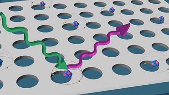
Alemán, a member of the UO’s Center for Optical, Molecular, and Quantum Science, has made artificial atoms that work in ambient conditions. The research, published in the journal Nano Letters, could be a big step in efforts to develop secure quantum communication networks and all-optical quantum computing.
“The big breakthrough is that we’ve discovered a simple, scalable way to nanofabricate artificial atoms onto a microchip, and that the artificial atoms work in air and at room temperature,” said Alemán, also a member of the UO’s Materials Science Institute.
“Our artificial atoms will enable lots of new and powerful technologies,” he said. “In the future, they could be used for safer, more secure, totally private communications, and much more powerful computers that could design life-saving drugs and help scientists gain a deeper understanding of the universe through quantum computation.”
Joshua Ziegler, a doctoral student researcher in Alemán’s lab, and colleagues drilled holes — 500 nanometers wide and four nanometers deep — into a thin two-dimensional sheet of hexagonal boron nitride, which is also known as white graphene because of its white color and atomic thickness.
To drill the holes, the team used a process that resembles pressure-washing, but instead of a water jet uses a focused beam of ions to etch circles into the white graphene. They then heated the material in oxygen at high temperatures to remove residues.
Using optical confocal microscopy, Ziegler next observed tiny spots of light coming from the drilled regions. After analyzing the light with photon counting techniques, he discovered that the individual bright spots were emitting light at the lowest possible level — a single photon at a time.
These patterned bright spots are artificial atoms and they possess many of the same properties of real atoms, like single photon emission.
With the success of the project, Alemán said, the UO is now ahead of the pack in efforts to develop such materials in quantum research. And that puts a smile on Alemán’s face.
When he joined the UO in 2013, he had planned to pursue the idea that artificial atoms could be created in white graphene. However, before Alemán could set his own research in motion, another university team identified artificial atoms in flakes of white graphene.
Alemán then sought to build on that discovery. Fabricating the artificial atoms is the first step towards harnessing them as sources of single particles of light in quantum photonic circuits, he said.
“Our work provides a source of single photons that could act as carriers of quantum information or as qubits. We’ve patterned these sources, creating as many as we want, where we want,” Alemán said. “We’d like to pattern these single photon emitters into circuits or networks on a microchip so they can talk to each other, or to other existing qubits, like solid-state spins or superconducting circuit qubits.”
Co-authors on paper were UO doctoral students Joshua Ziegler, Rachael Klaiss, Andrew Blaikie and David Miller, and Viva Horowitz, a professor of physics at Hamilton College in New York, who spent summer 2018 in Alemán’s lab as a visiting professor.
The National Science Foundation-supported research was done in Alemán’s lab, the UO’s Center for Advanced Materials Characterization in Oregon and the Oregon Rapid Materials Prototyping Facility. The latter was established in 2016 by an award from the M. J. Murdock Charitable Trust.
—By Jim Barlow, University Communications
Share on:


Subscribe
Stay ahead of the technologies shaping the future of electronics with our latest newsletter, Advanced Electronics Packaging Digest. Get expert insights on advanced packaging, materials, and system-level innovation, delivered straight to your inbox.
Subscribe now to stay informed, competitive, and connected.
Suggested Items
AI Demand Drives PCB Material Market Growth
05/08/2026 | TPCAAs AI computing continues to drive a comprehensive upgrade in hardware specifications, the global printed circuit board industry is undergoing a profound structural transformation.
I-Connect007 Editor’s Choice: Five Must-Reads for the Week
05/01/2026 | Michelle Te, I-Connect007If it feels like the PCB industry is accelerating faster than ever, you’re not imagining it. From advanced materials driven by AI applications to renewed investment in domestic manufacturing—and the next generation stepping into critical roles—there’s a lot shifting at once. My selections for this week highlight where the pressure points are forming, and where the opportunities are emerging.
Electronics Manufacturing Needs Your Voice: Global Sentiment Survey Now Live
04/30/2026 | Global Electronics AssociationThe latest monthly Global Sentiment Survey from the Global Electronics Association is now open. At a time when demand uncertainty, policy shifts, energy costs, and supply chain recalibration are pulling the industry in multiple directions, the survey captures something macroeconomic data often misses: how manufacturers are actually experiencing conditions on the ground.
From Backbone to Breakthroughs: I-Connect007 Wraps PCB Materials Series with Focus on Innovation
05/06/2026 | I-Connect007I-Connect007 wraps up its six-part podcast series, PCB Materials: The Backbone and Future of Electronics, with Episode 6 and a discussion focusing on innovation. In Episode 6, Marcy LaRont speaks with Isola CTO Kirk Thompson about a critical turning point for the PCB industry as innovation accelerates. As data rates climb and demands from AI infrastructure, power density, flexible electronics, photonics, and chiplet integration intensify, traditional material assumptions are no longer sufficient.
Jiva Soluboard Getting the Attention It Deserves
04/30/2026 | Marcy LaRont, I-Connect007 MagazineJiva is a newer company that bridges the divide between PCB fabrication and product circularity or sustainability. Jiva Soluboard is the first fully recyclable laminate material ever created for PCB fabrication, and it's not going unnoticed. Stephen Driver, CEO of Jiva, gave us an update at APEX EXPO, including an exciting certification achievement in February.