


 Beyond the Board: What Companies Need to Know Before Entering the MilAero PCB Market
 Defense Speak Interpreted: If CHIPS Cuts Back, What Happens to Electronics Packaging Funds?
 American Made Advocacy: Where’s the Budget for a Modern Military Run on Microelectronics?


Laser Processing Method to Increase Efficiency of Optoelectronic Devices
April 15, 2019 | NRLEstimated reading time: 2 minutes
Scientists at the U.S. Naval Research Laboratory (NRL) discovered a new method to passivate defects in next generation optical materials to improve optical quality and enable the miniaturization of light emitting diodes and other optical elements.
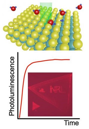
Image Caption: (Top) Illustration of a water molecule bonding at a sulfur vacancy in the MoS2 upon laser light exposure. (Bottom) Photoluminescence (PL) increase observed during laser light exposure in ambient. (Inset) Fluorescence image showing brightened regions spelling out “NRL.” (U.S. Naval Research Laboratory)
“From a chemistry standpoint, we have discovered a new photocatalytic reaction using laser light and water molecules, which is new and exciting,” said Saujan Sivaram, Ph.D., lead author of the study. “From a general perspective, this work enables the integration of high quality, optically active, atomically thin material in a variety of applications, such as electronics, electro-catalysts, memory, and quantum computing applications.”
The NRL scientists developed a versatile laser processing technique to significantly improve the optical properties of monolayer molybdenum disulphide (MoS2)—a direct gap semiconductor—with high spatial resolution. Their process produces a 100-fold increase in the material’s optical emission efficiency in the areas “written” with the laser beam.
According to Sivaram, atomically thin layers of transition metal dichalcogenides (TMDs), such as MoS2, are promising components for flexible devices, solar cells, and optoelectronic sensors due to their high optical absorption and direct band gap.
“These semiconducting materials are particularly advantageous in applications where weight and flexibility are a premium,” he said. “Unfortunately, their optical properties are often highly variable and non-uniform making it critical to improve and control the optical properties of these TMD materials to realize reliable high efficiency devices.”
“Defects are often detrimental to the ability of these monolayer semiconductors to emit light,” Sivaram said. “These defects act as non-radiative trap states, producing heat instead of light, therefore, removing or passivating these defects is an important step towards high efficiency optoelectronic devices.”
In a traditional LED, approximately 90% of the device is a heat sink to improve cooling. Reduced defects enable smaller devices to consume less power, which results in a longer operational lifetime for distributed sensors and low-power electronics.
The researchers demonstrated that water molecules passivate the MoS2 only when exposed to laser light with an energy above the band gap of the TMD. The result is an increase in photoluminescence with no spectral shift.
Treated regions maintain a strong light emission compared to the untreated regions that exhibit much a weaker emission. This suggest that the laser light drives a chemical reaction between the ambient gas molecules and the MoS2.
“This is a remarkable achievement,” said Berend Jonker, Ph.D., senior scientist and principal investigator. “The results of this study pave the way for the use of TMD materials critical to the success of optoelectronic devices and relevant to the Department of Defense mission.”
Share on:


Testimonial
"We’re proud to call I-Connect007 a trusted partner. Their innovative approach and industry insight made our podcast collaboration a success by connecting us with the right audience and delivering real results."
Julia McCaffrey - NCAB GroupSuggested Items
September 2025 PCB007 Magazine: The Future of Advanced Materials
09/16/2025 | I-Connect007 Editorial TeamMoore’s Law is no more, and the advanced material solutions being developed to grapple with this reality are surprising, stunning, and perhaps a bit daunting. Buckle up for a dive into advanced materials and a glimpse into the next chapters of electronics manufacturing.
I-Connect007 Launches Advanced Electronics Packaging Digest
09/15/2025 | I-Connect007I-Connect007 is pleased to announce the launch of Advanced Electronics Packaging Digest (AEPD), a new monthly digital newsletter dedicated to one of the most critical and rapidly evolving areas of electronics manufacturing: advanced packaging at the interconnect level.
Panasonic Industry will Double the Production Capacity of MEGTRON Multi-layer Circuit Board Materials Over the Next Five Years
09/15/2025 | Panasonic Industry Co., Ltd.Panasonic Industry Co., Ltd., a Panasonic Group company, announced plans for a major expansion of its global production capacity for MEGTRON multi-layer circuit board materials today. The company plans to double its production over the next five years to meet growing demand in the AI server and ICT infrastructure markets.
Trouble in Your Tank: Implementing Direct Metallization in Advanced Substrate Packaging
09/15/2025 | Michael Carano -- Column: Trouble in Your TankDirect metallization systems based on conductive graphite are gaining popularity throughout the world. The environmental and productivity gains achievable with this process are outstanding. Direct metallization reduces the costs of compliance, waste treatment, and legal issues related to chemical exposure. A graphite-based direct plate system has been devised to address these needs.
Fresh PCB Concepts: Designing for Success at the Rigid-flex Transition Area
08/28/2025 | Team NCAB -- Column: Fresh PCB ConceptsRigid-flex PCBs come in all shapes and sizes. Manufacturers typically use fire-retardant, grade 4 (FR-4) materials in the rigid section and flexible polyimide materials in the flex region. Because of the small size, some rigid-flex PCBs, like those for hearing aid devices, are among the most challenging to manufacture. However, regardless of its size, we should not neglect the transition area between the rigid and flexible material.