


 The Chemical Connection: Onshoring PCB Production—Daunting but Certainly Possible
 It’s Only Common Sense: The Phone Is Still Mightier Than the Keyboard


Tuning Terahertz Transmission
April 18, 2019 | A*STAREstimated reading time: 3 minutes
The ability to manipulate light on a subwavelength-scale could lead to a revolution in photonic devices such as antennas, solar panels, and even cloaking devices. Nanotechnology advances have made this possible through the development of metasurfaces, materials covered in features smaller than the wavelength of the light.
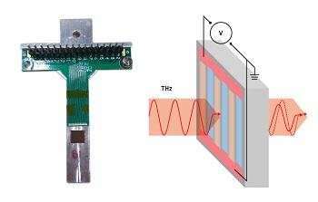
(left) A mounted device including the new tunable metasurface developed by Ding, Teng and co-workers. (right) When terahertz radiation hits the surface of interlinked p-type and n-type semiconducting silicon fingers, the amount of radiation reflected and transmitted can be controlled precisely using an applied voltage.
Now, a team led by A*STAR researchers has produced a highly promising metasurface that can be precisely controlled using a conventional electrical circuit so that it reflects and transmits different amounts of radiation. It can even reach the condition of ‘perfect antireflection’ where it reflects no radiation at all. Specifically, the surface works with broadband terahertz radiation, which is found at the far end of the infrared spectrum and has many potential uses, particularly in security or medical fields.
“Terahertz radiation can penetrate a wide variety of non-conducting materials, but is blocked by liquid water or metals,” explains Lu Ding, who led the work with Jinghua Teng at the A*STAR Institute of Materials Research and Engineering (IMRE). “This means that terahertz beams can be used for material characterization, layer inspection, and producing high-resolution images of the interior of solid objects. It is non-ionizing radiation, and safer than X-rays.”
Previous metasurfaces have been designed to manipulate the reflection of terahertz radiation. However, their application has been limited, as Ding explains: “Conventional terahertz antireflection surfaces are passive and often employ an ultrathin metal coating that, once fabricated, becomes fixed and you can’t actively tune its performance.”
“An electrically tunable metasurface would produce more versatile devices and render more flexibility in system design,” adds Teng. “It is the breakthrough the community is looking for.”
Ding and Teng, along with coworkers at the A*STAR Institute of Microelectronics (IME), Nanyang Technological University, National University of Singapore and Jilin University in China, fabricated their new metasurface on a silicon wafer, using a process entirely compatible with the complementary metal–oxide semiconductor (CMOS) technologies that underpin most electronics.
The exposed metasurface contains stripes of semiconducting silicon, doped with other elements. These stripes are alternately n-type, in which the moving charge carriers are electrons, and p-type, in which the carriers are positively-charged ‘holes’ in the electron structure. When the voltage supplied to the p-n junctions is changed, the reflection and transmission of the radiation also change.
The team realized that the reflection coefficient increased in response to a temperature rise caused by the applied voltage. Meanwhile, the transmission showed a more complex response depending on the voltage polarity, which affected the type of charge carrier that became dominant. Using terahertz time-domain spectroscopy, the team showed that certain voltage conditions caused the echo pulse from the metasurface to vanish, representing complete antireflection.
As well as providing this unprecedented control over reflection and transmission, the metasurface has the benefit of being almost entirely flat at an atomic level. This makes it ideal for building up smooth layers in more complex devices.
“Another big advantage is for our research looking into how 2D materials interact with 2D metamaterials or metasurfaces, a topic in our project in A*STAR’s 2D Semiconductors Pharos Program,” says Teng. “The atomically smooth surface makes the transfer and formation of 2D-Si heterostructures much easier than the patterned surfaces of nano-sized pillars or disks seen on conventional metasurfaces.”
“We could further exploit this type of metasurface by independently biasing the p-n junctions or designing modular functions, meaning that we would have pre-programmable metamaterials,” says Ding. Teng adds that the same platform could be used for studying promising 2D materials like molybdenum disulfide, which exhibits impressive electronic and optical properties for use in new flexible circuits.
Share on:


Testimonial
"Our marketing partnership with I-Connect007 is already delivering. Just a day after our press release went live, we received a direct inquiry about our updated products!"
Rachael Temple - AlltematedSuggested Items
ITW EAE Despatch Ovens Now Support ASTM 5423 Testing
10/15/2025 | ITW EAEAs the demand for high-performance electrical insulation materials continues to grow—driven by the rapid expansion of electric vehicles (EVs) and energy storage systems—thermal processing has become a critical step in material development.
Beyond Thermal Conductivity: Exploring Polymer-based TIM Strategies for High-power-density Electronics
10/13/2025 | Padmanabha Shakthivelu and Nico Bruijnis, MacDermid Alpha Electronics SolutionsAs power density and thermal loads continue to increase, effective thermal management becomes increasingly important. Rapid and efficient heat transfer from power semiconductor chip packages is essential for achieving optimal performance and ensuring long-term reliability of temperature-sensitive components. This is particularly crucial in power systems that support advanced applications such as green energy generation, electric vehicles, aerospace, and defense, along with high-speed computing for data centers and artificial intelligence (AI).
Is Glass Finally Coming of Age?
10/13/2025 | Nolan Johnson, I-Connect007Substrates, by definition, form the base of all electronic devices. Whether discussing silicon wafers for semiconductors, glass-and-epoxy materials in printed circuits, or the base of choice for interposers, all these materials function as substrates. While other substrates have come and gone, silicon and FR-4 have remained the de facto standards for the industry.
Creative Materials to Showcase Innovative Functional Inks for Medical Devices at COMPAMED 2025
10/09/2025 | Creative Materials, Inc.Creative Materials, a leading manufacturer of high-performance functional inks and coatings, is pleased to announce its participation in COMPAMED 2025, taking place November 17–20 in Düsseldorf, Germany.
Jiva Leading the Charge Toward Sustainable Innovation
09/30/2025 | Marcy LaRont, PCB007 MagazineEnvironmental sustainability in business—product circularity—is a high priority these days. “Circularity,” the term meant to replace “recycling,” in its simplest definition, describes a full circle life for electronic products and all their elements. The result is re-use or a near-complete reintroduction of the base materials back into the supply chain, leaving very little left for waste. For what cannot be reused productively, the ultimate hope is to have better, less harmful means of disposal and/or materials that can seamlessly and harmlessly decompose and integrate back into the natural environment. That is where Jiva and Soluboard come in.