


 Dan’s Biz Bookshelf: ‘Abundance: How We Build a Better Future’
 Trouble in Your Tank: In Complex Systems, Design Rules Aren’t Optional
 It’s Only Common Sense: The Phone Is Still Your Competitive Advantage


Inorganic Perovskite Absorbers for Use in Thin-Film Solar Cells
April 30, 2019 | HZBEstimated reading time: 2 minutes
A team at the Helmholtz Center Berlin has succeeded in producing co-evaporation of inorganic perovskite thin films at moderate temperatures - no post-heat treatment at high temperatures is necessary.
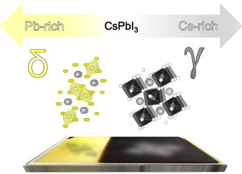
Image Caption: By coevaporation of cesium iodide and lead iodide, thin layers of CsPbI 3 can be prepared even at moderate temperatures. A cesium excess leads to stable perovskite phases. Copyright: J. Marquez-Prieto / HZB
As a result, it is much easier to produce thin-film solar cells made of this material. Inorganic perovskites are more thermally stable than the hybrid organometallic perovskites.
Teams around the world are working hard to develop perovskite solar cells. The focus is on so-called metalorganic hybrid perovskites, whose crystal structure is composed of both inorganic elements such as lead and iodine and an organic molecule.
Fully inorganic perovskite semiconductors such as CsPbI3 have the same crystalline architecture as hybrid perovskites, but contain an alkali metal such as cesium instead of an organic molecule. This makes them much more stable than hybrid perovskites but usually requires a very high temperature manufacturing step of several hundreds of degrees Celsius. For this reason, it has been difficult to integrate inorganic perovskite semiconductors into thin-film solar cells that can not tolerate high temperatures. Now it's a team around Dr. Thomas Unold succeeded in producing inorganic perovskite semiconductors at moderate temperatures so that they could also be used in various thin-film cells in the future.
For this, the physicists designed an innovative experiment that allowed them to synthesize and analyze many combinations of materials within a single sample. Co-evaporation of cesium iodide and lead iodide produced thin layers of CsPbI3, systematically varying the excess of elements in the atmosphere. The substrate temperature was below 60 degrees Celsius.
"Such a combinatorial approach will allow finding optimal manufacturing parameters for new material systems much faster than the traditional approach, which typically requires 100 samples to be made for 100 compositions," explains Unold. Through careful analysis during the synthesis and subsequent measurements of the optoelectronic properties, they were able to determine how the composition of the thin film affects the material properties.
Their measurements show that both the structural and important optoelectronic material properties are sensitive to the ratio between cesium and lead. Thus, a cesium excess allows a stable perovskite phase with good mobility and lifetime of the charge carriers.
In collaboration with the junior research group of Prof. Steve Albrecht at HZB, these optimized CsPbI3 layers demonstrated perovskite solar cells with an efficiency of more than 12% and a stability of more than 1200 hours. "We have shown that even inorganic perovskite absorbers could be suitable for use in thin-film solar cells, if they can be produced accordingly. We currently assume that such components can still be optimized very strongly," says Unold.
Share on:


Subscribe
Stay ahead of the technologies shaping the future of electronics with our latest newsletter, Advanced Electronics Packaging Digest. Get expert insights on advanced packaging, materials, and system-level innovation, delivered straight to your inbox.
Subscribe now to stay informed, competitive, and connected.
Suggested Items
Global Electronics Association Expands Free Member Training Library with New Safety and Ergonomics Courses
04/23/2026 | Global Electronics AssociationThe Global Electronics Association today announced three new complimentary courses in safety and ergonomics, expanding its member training library to help manufacturers onboard workers faster and improve production performance.
An Interview With Keynote Speaker Zack Kass on the 'AI Renaissance'
04/23/2026 | Marcy LaRont, I-Connect007Zack Kass is an AI evangelist, technologist, businessman, and the author of The Next Renaissance: AI and the Expansion of Human Potential. He was a key player in bringing open AI to market and the keynote speaker at APEX EXPO 2026. Immediately following his presentation, I brought Zack to our booth, where we had a most eye-opening conversation about both the positive and negative impacts of artificial intelligence, and going beyond what’s “impossible.”
India’s Vasantha Advanced Systems: EMS Success for 30 Years
04/22/2026 | Marcy LaRont, I-Connect007Based in one of India’s premier manufacturing regions, Vasantha Advanced Systems is an EMS provider that has built a reputation for quality, reliability, and long-term customer partnerships, earning repeated recognition from the Indian government through its National MSME Awards. Now, with a full spectrum of capabilities spanning PCB assembly, box build, and wire harness, and a workforce of more than 500, Vasantha is expanding its presence into the U.S. market. At APEX EXPO, I met Dr. Chidambaranathan and learned how this rising global player is positioning itself to meet the evolving needs of North American customers.
Mexico’s Wire Harness Pivot Point
04/22/2026 | Nolan Johnson, SMT007 MagazineMexico is a major producer of wire harnesses, but recent U.S. economic policies and Mexico’s domestic issues have had a ripple effect on the industry. Jesus Duarte, vice president of Mexico Assembly Wire Technology and president of Expo Wire Tech, explains the issue in greater depth and how the wire harness industry should respond on its own, rather than just reflect what Tier 1s are doing.
Flexible Thinking: Designing Flex Circuits for Dynamic Reliability
04/09/2026 | Joe Fjelstad -- Column: Flexible ThinkingFlex circuits flex. No surprises there. However, they are also very commonly designed into products because they are thin and offer consistent thickness and dielectric properties, attributes highly prized by present-day product designers of personal electronics. This would include smartphones and, increasingly, wearable electronics for medical monitoring and even fashion.