


 Driving Innovation: Mechanical and Optical Processes During Rigid-flex Production
 It’s Only Common Sense: Your Biggest Competitor Is Complacency
 The Chemical Connection: Onshoring PCB Production—Daunting but Certainly Possible


Researchers Create ‘Force Field’ for Super Materials
May 9, 2019 | University of SurreyEstimated reading time: 1 minute
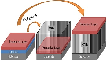
When curved and rolled into cylinders, thin graphene layers form CNT structures which can be a thousandth of the diameter of human hair. Both graphene and CNTs possess extraordinary properties such as extreme electrical conduction, or 100 times the strength of high tensile steel. Although widely regarded as the key to developing various future technologies such as batteries and supercapacitor, growth of graphene and CNTs are plagued with environmental ‘poisoning’ to the catalyst which causes poor conductivity and reliability issues.
In a paper published by the journal Carbon, researchers from the University of Surrey detail their new method for covering the catalyst by using a protective layer that is configured to allow carbon diffusion and therefore can be used to protect the catalyst from environmental contamination. The technique allows the catalyst to be transported, stored or accurately calibrated for future use.
Professor Ravi Silva, Director of Advanced Technology Institute at the University of Surrey, said: “The protective catalyst technique provides a breakthrough in terms of usability and industrial applicability of carbon nanomaterials. For example, the poisoning of the catalyst by environmental contamination such as oxidation and unwanted etching of the thin catalyst film during reactive ion etching or wet-etching can now be prevented.”
Lead author of the study, Dr Muhammad Ahmad from the University of Surrey, said: “The age-old problem of poor attachment of the carbon nano-materials to the substrate has now been solved using this unique technique. By fine tuning the thickness of the protective layer, accurate control of the carbon supply to the catalyst is achieved to grow selected numbers of graphene layers or precise CNT films.”
“We hope that our research will free fellow scientists to unlock the incredible potential of carbon nanomaterials and I would not be surprised to see advances in areas such as sensor, battery and supercapacitor technologies in the very near future.”
Share on:


Testimonial
"In a year when every marketing dollar mattered, I chose to keep I-Connect007 in our 2025 plan. Their commitment to high-quality, insightful content aligns with Koh Young’s values and helps readers navigate a changing industry. "
Brent Fischthal - Koh YoungSuggested Items
Closing the Loop on PCB Etching Waste
09/09/2025 | Shawn Stone, IECAs the PCB industry continues its push toward greener, more cost-efficient operations, Sigma Engineering’s Mecer System offers a comprehensive solution to two of the industry’s most persistent pain points: etchant consumption and rinse water waste. Designed as a modular, fully automated platform, the Mecer System regenerates spent copper etchants—both alkaline and acidic—and simultaneously recycles rinse water, transforming a traditionally linear chemical process into a closed-loop system.
The Chemical Connection: Through-glass Vias in Glass Substrates
06/24/2025 | Don Ball -- Column: The Chemical ConnectionThis month’s theme is vias and how best to ensure via quality and reliability. I don’t have much expertise in this process area or much to contribute that most of you don’t already know. However, I’ve recently become peripherally involved in a via technology that may be of more than academic interest to some of us. It entails putting vias in a material not usually associated with PCB manufacturing: through-glass vias (TGVs) in glass substrates.
In Pursuit of Perfection: Defect Reduction—May 2025 PCB007 Magazine Now Available
05/15/2025 | I-Connect007 Editorial TeamFor bare PCB board fabrication, defect reduction is a critical aspect of a company's bottom line profitability. In the May 2025 issue of PCB007 Magazine, we examine the imaging, etching, and plating processes, as well as product traceability on the shop floor, providing information and insight into how you can reduce your defects and increase yields.
DuPont to Showcase Advanced Semiconductor Wet Etching Innovations at the Surface Preparation and Cleaning Conference
05/13/2025 | DuPontDuPont announced that it will present its latest developments in semiconductor wet etching technologies at the upcoming Surface Preparation and Cleaning Conference (SPCC) in Chandler, Arizona, beginning May 20.
The Chemical Connection: Common Misconceptions in Wet Processing
04/28/2025 | Don Ball -- Column: The Chemical ConnectionInitially, I thought an April Fool’s column would be fun this month. I could highlight some of the crazier ideas and misconceptions I’ve witnessed over the years from potential customers and we could all have a good laugh. For example, there was a first-time buyer of a ferric chloride etcher (with no regeneration system) who was astonished to learn that he had to put fresh etchant in the system occasionally to maintain production.