


 Dan’s Biz Bookshelf: ‘Abundance: How We Build a Better Future’
 Trouble in Your Tank: In Complex Systems, Design Rules Aren’t Optional
 It’s Only Common Sense: The Phone Is Still Your Competitive Advantage


Bring on Faster Internet: Device Packs More Into Optical Fibre
May 21, 2019 | University of QueenslandEstimated reading time: 2 minutes
A research team has developed a light beam device that could lead to faster internet, clearer images of space and more detailed medical imaging.
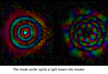
University of Queensland researcher and optical engineer Dr Joel Carpenter worked with Nokia Bell Labs to build the device to tackle the challenge of splitting light into the shapes it is made up of, known as modes.
“Splitting a beam of light into colours is easy because nature gives you that one for free—think of rainbows or when light shines through glass at an angle,” Dr Carpenter said.
“The mode sorter splits a light beam into modes, instead of pixels like a camera would, and this results in higher-quality imaging and communication.
“Our device performs a basic operation in physics, so it seemed a little strange to us that something like this did not already exist, as this topic had been investigated around the world for about 25 years.”
Study co-author Nicolas Fontaine of Nokia Bell Labs said the device could bring a number of benefits.
“Each of these modes can be its own independent channel of information, and with this device we can pack hundreds of modes into a single optical fibre,” Dr Fontaine said.
“This can greatly increase the amount of information that can travel through that fibre, leading to faster internet speeds for more people.
“We hope this device will aid many applications that work with light beams, due to its functionality and the relative simplicity with which it can be built.”
Dr Carpenter said the mode sorter could improve imaging quality, from small biomedical images to large astronomical images.
“Just as an image can be made by adding a bunch of pixels together, we can make an image or beam by adding together a bunch of these modes,” he said.
“Some things are easier to detect if you look at the modes rather than pixels, because it is displaying the image in a different form.
“For example, modes could make it easier to detect an image of a planet orbiting a far-away star.”
Share on:


Subscribe
Stay ahead of the technologies shaping the future of electronics with our latest newsletter, Advanced Electronics Packaging Digest. Get expert insights on advanced packaging, materials, and system-level innovation, delivered straight to your inbox.
Subscribe now to stay informed, competitive, and connected.
Suggested Items
Gregoire Outters Promoted to President of Teledyne Marine Group
04/06/2026 | TeledyneTeledyne Technologies Incorporated announced the promotion of Gregoire Outters to President of its Teledyne Marine Group.
Teledyne Strengthens Commitment to the Space Sector
04/01/2026 | BUSINESS WIRETeledyne Technologies Incorporated is excited to announce the integration of the company’s extensive portfolio of space-focused technologies and businesses, reinforcing its long-term commitment to the global space sector.
Teledyne to Supply Detectors for Lazuli Space Observatory
03/30/2026 | BUSINESS WIRETeledyne Space Imaging, part of Teledyne Technologies Incorporated has been awarded a contract by Schmidt Sciences to deliver advanced near-infrared (NIR) H4RG-10 flight focal plane arrays (FPAs) and custom electronics for integration into the Integral Field Spectrograph on the groundbreaking Lazuli Space Observatory.
New Superconducting Chip Could Enable Breakthrough Nondestructive Terahertz Imaging
03/23/2026 | University of GlasgowA tiny crystal chip which uses terahertz radiation to see clearly through a wide range of materials could find applications in healthcare, biological research, and security screening.
The Test Connection Adds Creative Electron Prime TruVision™ X-ray and CT System for Deeper Failure Analysis
03/05/2026 | TTCIThe Test Connection Inc. (TTCI), a trusted provider of electronic test and manufacturing solutions for more than 45 years, has added the Prime TruVision™ X-ray and computed tomography (CT) inspection system from Creative Electron to its engineering and analysis services.