


 The Right Approach: Get Ready for ISO 9001 Version 6
 Dan’s Biz Bookshelf: ‘Still Broke: Walmart’s Remarkable Transformation'
 Driving Innovation: Depth Routing Processes—Achieving Unparalleled Precision in Complex PCBs


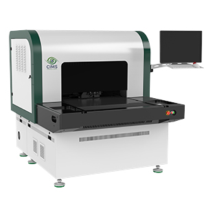
CIMS Debuts Through Laser Via Inspection Solution
May 28, 2019 | CIMSEstimated reading time: Less than a minute
Through laser via is a process of producing through-holes in ultra-high density PCB and IC substrates using laser drilling systems. This advanced process achieves much smaller diameter holes compared to traditional mechanical drilling.
The Galaxy VIA series is CIMS' latest solution for inspecting through laser via produced with this process. It is designed to detect all types of defects within the holes and control the narrowing down of the drill opening, sometimes referred to as via neck.
Galaxy VIA systems are equipped with brand new illumination called ViaLight, designed for transmissive light inspection to get the most accurate image of the interior of the holes.
The systems in the Galaxy VIA series are capable of inspecting through laser via drills as small as 20 microns in diameter, can detect undersize and oversize defects, contamination and debris inside, can identify plugged or missing holes as well as drill shifts beyond allowable tolerances.
Powerful statistical packages further extend capabilities of Galaxy VIA series providing real time process control used for laser drill tool calibration.
The Galaxy VIA 20μ model has been showcased during the last CTEX show in Suzhou, China.
Share on:


Testimonial
"Our marketing partnership with I-Connect007 is already delivering. Just a day after our press release went live, we received a direct inquiry about our updated products!"
Rachael Temple - AlltematedSuggested Items
Closing the Loop on PCB Etching Waste
09/09/2025 | Shawn Stone, IECAs the PCB industry continues its push toward greener, more cost-efficient operations, Sigma Engineering’s Mecer System offers a comprehensive solution to two of the industry’s most persistent pain points: etchant consumption and rinse water waste. Designed as a modular, fully automated platform, the Mecer System regenerates spent copper etchants—both alkaline and acidic—and simultaneously recycles rinse water, transforming a traditionally linear chemical process into a closed-loop system.
The Chemical Connection: Experience and Wisdom Gained by Doing Business
09/03/2025 | Don Ball -- Column: The Chemical ConnectionA well-managed company learns to adjust its strategies and processes based on what it learns during challenging times. The experience gained from making (or losing) a difficult sale is invaluable in adapting new sales and manufacturing processes necessary to make that sale the next time, no matter how painful those new processes might be.
MacDermid Alpha Awarded for Innovation: Driving Process Optimization and Efficiency with Major Indian EMS Provider
08/28/2025 | MacDermid Alpha Electronics SolutionsMacDermid Alpha Electronics Solutions, a leading global supplier of integrated materials for the electronics industry, is recognized by one of India’s top EMS providers, Syrma SGS, with an award for innovation that advanced process optimization, enhanced operational efficiency, and yield gains.
Partnerships Drive Innovation for a Brighter Manufacturing Future
08/26/2025 | Barry Matties, I-Connect007When Schweitzer Engineering Laboratories (SEL) opened its greenfield facility in 2023, it did so with careful attention to choosing its suppliers. In this discussion, Collin Peters, electronics business director for North America at MKS’ Atotech, and Justin Kennedy, manager of engineering at SEL, explore their unique partnership that includes collaborative efforts to develop innovative solutions like the Uniplate® PLBCu6 line.
The Art and Science of PCB Floor Planning: A Comprehensive Guide
08/14/2025 | Cory Grunwald and Jeff Reinhold, Monsoon SolutionsPCB design is an intricate and crucial part of developing electronic products. One of the foundational stages of PCB design is floor planning, a phase where the placement of components and the flow of signals are meticulously mapped out. A good floor plan ensures that the PCB performs well, is easy to manufacture, and meets all mechanical and electrical requirements. We’ll explore the essential aspects of floor planning, from its objectives and process to the challenges that designers face.