


 The Marketing Minute: Marketing With Layers
 The Right Approach: Electro-Tek—A Williams Family Legacy, Part 1
 It’s Only Common Sense: If You’re Not Differentiated, You’re Dead


Imperfection is OK for Better MOFs
May 28, 2019 | KAUSTEstimated reading time: 2 minutes
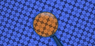
Perfect crystals are not necessarily the most useful. Defects in the ordered crystalline structure of metal-organic frameworks (MOFs) could tailor these versatile materials for specific applications. KAUST researchers have already developed a pioneering method to image the defects using transmission electron microscopy. They now report that creating specific defects, visualizing them, and investigating their chemical effects takes the exploration of MOFs to new levels of detail and control.
MOFs contain regularly spaced metallic clusters connected by carbon-based organic linker groups. Varying the metals in the clusters and the structure of the linkers creates a huge diversity of MOFs with varying pore networks and different chemical properties. Two of the major applications MOFs are being developed for are for use as catalysts and as highly selective gas adsorption and separation materials.
MOFs are one of the hottest areas of chemical research, and KAUST scientists are hard at work to remain in the forefront. The latest advance builds on a long record of discoveries and has involved three KAUST research centers, the KAUST Core labs and collaborators in China and the UK.
"The biggest surprise we are revealing is that there are diverse defects in almost all MOFs, even those that were previously considered to be perfect," says researcher, Yu Han of the KAUST Advanced Membranes and Porous Materials Center.
Han explains that investigating the defects is challenging because MOF crystals are fragile and easily damaged by the electron beams used in conventional electron microscopy. The KAUST team has overcome this problem by using a highly sensitive electron-counting camera, combined with a suite of specially designed image processing methods.
This new ability to peer directly into a MOF at a high level of resolution reveals that two types of defects can coexist, due to missing metallic clusters and missing linkers. "Such details could not be seen prior to our work," says Han.
The researchers also explored creating defects in MOFs with chemical treatment and monitoring how the pattern of defects develops. This demonstrates the potential to fine tune the defects to manipulate the chemical properties of a MOF.
The KAUST team has demonstrated the power of this strategy by finding that a specific MOF with missing cluster defects is more catalytically active than one with missing linker defects.
The researchers are now working to further refine their imaging technique and to apply it to larger crystals. "We hope to disclose more unknowns about MOFs in order to optimize their applications," says Han.
Share on:


Testimonial
"We’re proud to call I-Connect007 a trusted partner. Their innovative approach and industry insight made our podcast collaboration a success by connecting us with the right audience and delivering real results."
Julia McCaffrey - NCAB GroupSuggested Items
Smart Eye Collaborates with Sony on Next-Generation Interior Sensing and Iris Authentication
10/09/2025 | Smart EyeSmart Eye AB, the global leader in Interior Sensing AI and Driver Monitoring Systems (DMS), announced a collaboration with Sony Semiconductor Solutions Corporation (Sony) to integrate Smart Eye’s interior sensing and biometric authentication software with Sony’s newly released IMX775 RGB-IR image sensor.
SEMICON Europa 2025 to Highlight Innovations in Advanced Packaging, Fab Management, and MEMS and Imaging Sensors to Bolster Europe’s Semiconductor Resilience
10/03/2025 | SEMISemiconductor industry experts will convene at SEMICON Europa 2025, November 18-21 at Messe München in Munich, to explore the latest trends and innovations in advanced packaging and fab management.
MEMS & Imaging Sensors Summit to Spotlight Sensing Revolution for Europe’s Leadership
09/11/2025 | SEMIIndustry experts will gather November 19-20 at the SEMI MEMS & Imaging Sensors Summit 2025 to explore the latest breakthroughs in AI-driven MEMS and imaging optimization, AR/VR technologies, and advanced sensor solutions for critical defence applications.
Direct Imaging System Market Size to Hit $4.30B by 2032, Driven by Increasing Demand for High-Precision PCB Manufacturing
09/11/2025 | Globe NewswireAccording to the SNS Insider, “The Direct Imaging System Market size was valued at $2.21 Billion in 2024 and is projected to reach $4.30 Billion by 2032, growing at a CAGR of 8.68% during 2025-2032.”
I-Connect007’s Editor’s Choice: Five Must-Reads for the Week
07/04/2025 | Marcy LaRont, I-Connect007For our industry, we have seen several bullish market announcements over the past few weeks, including one this week by IDC on the massive growth in the global server market. We’re also closely watching global trade and nearshoring. One good example of successful nearshoring is Rehm Thermal Systems, which celebrates its 10th anniversary in Mexico and the official opening of its new building in Guadalajara.