


 Dan’s Biz Bookshelf: ‘Abundance: How We Build a Better Future’
 Trouble in Your Tank: In Complex Systems, Design Rules Aren’t Optional
 It’s Only Common Sense: The Phone Is Still Your Competitive Advantage


Quantum Communication: Making Two From One
June 7, 2019 | MAX-PLANCK-GESELLSCHAFTEstimated reading time: 3 minutes
In the future, quantum physics could become the guarantor of secure information technology. To achieve this, individual particles of light—photons—are used for secure transmission of data. Findings by physicists from the Max Planck Institute for Solid State Research could play a key role. The researchers accidentally came across a light source that generates a photon pair from the energy of an electron. One of these particles of light has the potential to serve as a carrier of the fragile quantum information, the other, as a messenger to provide prior notification of its twin.
In contrast to quantum communication, a cook has the luxury of being able to look if all the ingredients he or she needs for a recipe are in the cupboard. After all, flour doesn’t go bad the moment you glance at it. A physicist trying to test whether a procedure to transmit quantum information has worked as planned is in a much trickier position. Quantum objects change their state when they are observed, i.e. measured. In quantum communication, this makes it difficult to control the information transmitted by photons. But that’s the critically important point. Every contact with the environment can destroy the quantum information transported by photons, and in addition, sources of individual light particles often generate single photons only very irregularly. Just how do you guarantee a photon is on its way without measuring it? Pairs of photons are the solution. One photon might be able to serve as a messenger for its twin.
An Unexpected Source of Photon Pairs
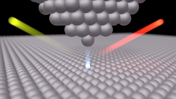
Scientists at the Max Planck Institute for Solid State Research have now discovered an unexpected source of such photon pairs: a scanning tunnelling microscope. Researchers normally use a microscope of this kind to study the surfaces of conducting or semiconducting materials. The microscope is based on an effect known as quantum tunnelling. This describes how electrons have a certain probability of passing through a barrier which, according to classical physics, they would not normally be able to cross. In a scanning tunnelling microscope, a voltage is applied to a metallic tip, causing electrons to tunnel over a short distance to a sample. If an electron loses energy during this tunnelling process, light is produced.
It is precisely this light that the Stuttgart physicists have been investigating for a number of years. Their work has now led to a surprising observation: during tunnelling, in addition to individual light particles, photon pairs are also formed, at a rate 10,000 times higher than theory predicts. "According to theory, the probability of a photon pair forming is so low that we should never see it," explains scientist Christopher Leon. "But our experiment shows that photon pairs are being generated at a much higher rate. That was a huge surprise for us."
The physicists measured the photon pairs using two detectors, allowing them to measure the interval of time between the arriving photons. "At the moment when a photon pair forms in a tunnelling junction, they are less than 50 trillionths of a second apart," explains the leading scientist Klaus Kuhnke. For now, it is impossible to say whether the photons are actually produced simultaneously or in rapid succession. The resolution of the detectors is not yet high enough.
New Applications for Tunnelling Junctions
The findings open up new applications in photonics and quantum communication for tunnelling junctions. Scientists do already know of processes that generate photon pairs, but most of them employ intense laser light. In contrast, the method developed by the Max Planck scientists in Stuttgart is purely electronic.
In addition, the required components are very small, and the process takes place on an atomic scale. This means the new light source could also be used in future generations of computer chips, replacing electronic components with optical ones. One advantage of employing photons is that they promise fast and lossless data transmission. The photon pairs in the experiment carried out by the Stuttgart researchers were extremely fast, but the ultra-high vacuum and the very low temperatures required by the experiment remain a practical challenge.
The next step for the scientists is to find out whether measuring one photon directly affects the state of the other. If so, the light particles would be entangled. Entangled particles of this kind are crucial in quantum cryptography. The results also raise fundamental questions about how photon pairs are formed. Until now, the process has been all but overlooked from a theoretical background. "The fact that photon pairs are generated indicates that a complicated process must be taking place," says theorist Olle Gunnarsson. Klaus Kern, Director of the Max Planck Institute for Solid State Research, agrees that the process is exciting: “It's thrilling because it opens up a new perspective on how light is produced.”
Share on:


Subscribe
Stay ahead of the technologies shaping the future of electronics with our latest newsletter, Advanced Electronics Packaging Digest. Get expert insights on advanced packaging, materials, and system-level innovation, delivered straight to your inbox.
Subscribe now to stay informed, competitive, and connected.
Suggested Items
TLT Electronics Officially Opens Facility in Vietnam
05/06/2026 | TLT ElectronicsLithuanian EMS provider TLT Electronics has recently announced the opening of a new facility in Vietnam. For their clients, this is a chance to expand manufacturing into a second region without the headache of onboarding a new supplier. Same team, same processes, same quality standards — still TLT Manufacturing, just on another continent.
Trouble in Your Tank: In Complex Systems, Design Rules Aren’t Optional
05/06/2026 | Michael Carano -- Column: Trouble in Your TankThere is no question that the electronics industry, especially in circuit board design and fabrication, advanced packaging, and innovation throughout the value chain, has seen a significant transformation, whether it be in materials, system architecture, HDI and ultra HDI, semiconductors, or chiplets. AI and high-performance computing (HPC) are driving change across several fronts, including material properties, assembly techniques (think hybrid bonding), and power management.
Meet Emerging Engineers: Patrick Owen and Eric Mickenbecker, Summit Interconnect
05/05/2026 | Michelle Te, I-Connect007Patrick Owen and Eric Mickenbecker both work for Summit Interconnect, and are in their second year of the Global Electronics Association’s Emerging Engineer Program with mentor Brian Chislea. They stopped by the I-Connect007 booth at APEX EXPO and shared a bit of their story with me. Patrick has worked at the Hollister, California, plant since 2018, while Eric has been at the Chicago site since 2023. Like many of their peers, they came to the electronics industry from different paths, but are both excited about making an impact.
The Missing Connection: Wire Harness Quoting Joins the Digital Age
05/01/2026 | Joanne Harris, Tech-2marketingWalk the floor of a modern wire harness manufacturing facility, and the investment in technology is hard to miss. Automated wire cutting and stripping machines process thousands of cuts an hour with sub-millimeter precision. Computerized crimping presses deliver consistent, validated terminations that a hand tool never could. Laser wire markers, automated test benches, and vision-guided assembly stations represent hundreds of thousands of dollars of capital investment, all in service of building a better harness faster and more reliably than the competition.
EDADOC: Building the ‘Neural Hub’ for High-Compute Chips Within a Compact Space
04/28/2026 | ECIOEvery chip to the market must pass a stringent checkpoint before shipment known as ATE testing. Serving as the physical “neural hub” that connects test equipment worth millions of dollars with the device under test, the performance of the ATE test board directly determines the accuracy, efficiency, and final yield of chip testing. Amid the rapid rise of high-compute chips, what extreme challenges is this seemingly small circuit board facing? How is EDADOC addressing industry pain points through its one-stop “design + manufacturing” model?