


 Dan’s Biz Bookshelf: ‘Abundance: How We Build a Better Future’
 Trouble in Your Tank: In Complex Systems, Design Rules Aren’t Optional
 It’s Only Common Sense: The Phone Is Still Your Competitive Advantage


Iphone Plus Nanoscale Porous Silicon Equals Cheap, Simple Home Diagnostics
June 12, 2019 | Vanderbilt UniversityEstimated reading time: 2 minutes
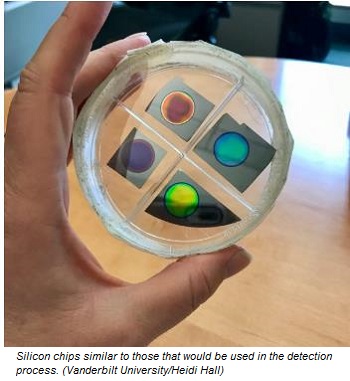
The simplest home medical tests might look like a deck of various silicon chips coated in special film, one that could detect drugs in the blood, another for proteins in the urine indicating infection, another for bacteria in water and the like. Add the bodily fluid you want to test, take a picture with your smart phone, and a special app lets you know if there’s a problem or not.
That’s what electrical engineer Sharon Weiss, Cornelius Vanderbilt Professor of Engineering at Vanderbilt University, and her students developed in her lab, combining their research on low-cost, nanostructured thin films with a device most American adults already own. “The novelty lies in the simplicity of the basic idea, and the only costly component is the smart phone,” Weiss said.
“Most people are familiar with silicon as being the material inside your computer, but it has endless uses,” she said. “With our nanoscale porous silicon, we’ve created these nanoscale holes that are a thousand times smaller than your hair. Those selectively capture molecules when pre-treated with the appropriate surface coating, darkening the silicon, which the app detects.”
Similar technology being developed relies on expensive hardware that compliments the smart phone. Weiss’ system uses the phone’s flash as a light source, and the team plans to develop an app that could handle all data processing necessary to confirm that the film simply darkened with the adding of fluid. What’s more, in the future, such a phone could replace a mass spectrometry system that costs thousands of dollars. The Transportation Security Administration owns hundreds of those at airports across the country, where they’re used to detect gunpowder on hand swabs.
Other home tests rely on a color change, which is a separate chemical reaction that introduces more room for error, Weiss said.
Weiss, Ph.D. student Tengfei Cao, and their team used a biotin-streptavidin protein assay and an iPhone SE, model A1662, to test their silicon films and found the accuracy to be similar to that of benchtop measurement systems. They also used a 3D printed box to stabilize the phone and get standardized measurements for the paper, but Weiss said that wouldn’t be necessary if further research and development led to a commercialized version.
Share on:


Subscribe
Stay ahead of the technologies shaping the future of electronics with our latest newsletter, Advanced Electronics Packaging Digest. Get expert insights on advanced packaging, materials, and system-level innovation, delivered straight to your inbox.
Subscribe now to stay informed, competitive, and connected.
Suggested Items
SMTA Ultra HDI Symposium, Day 1: AI at the Core or Out of the Game
04/13/2026 | Marcy LaRont, I-Connect007It was a beautiful 81°F morning in Arizona last Wednesday as I headed to the third annual SMTA Ultra HDI Symposium, focused on AI and ultra high density interconnect technology. Strategically held as part of Arizona’s Tech Week, this year’s conference took place in Avondale in Phoenix's West Valley. The event moved from the cozy offices of the Peoria Sports Complex (which paid homage to baseball’s spring training world) to the larger Avondale Conference Center, highlighting the importance of this area for electronics manufacturing investment.
PCBAA Sets Its Priorities for 2026: Support in the House and Senate
02/03/2026 | Marcy LaRont, I-Connect007David Schild, executive director of the Printed Circuit Board Association of America (PCBAA), leads an organization focused on the domestic manufacture of PCBs and substrates to support America’s critical microelectronics supply. In the continuation of this interview, David talks about the ways his organization is aligning its priorities with Washington, in particular, the Executive Branch. It might feel like a snail’s pace, but progress could mean financial support and more domestic security, even for the smaller companies.
SMT Perspectives & Prospects: Artificial Intelligence Part 6: Data Module 1
10/07/2025 | Dr. Jennie Hwang -- Column: SMT Perspectives and ProspectsData is one of the six pillars of AI infrastructure. It is critical to the performance of artificial intelligence (AI) models. AI data, essential to both the training and inference of Generative AI models, connotes the datasets used to train, validate, and test AI models. Training data provides models with a frame of reference by establishing a baseline against which models can compare new data using pre-trained models for predictions or generating new content.
U.S. Uses Secret Trackers to Trace AI Chips Diverted to China, Sources Say
08/18/2025 | I-Connect007 Editorial TeamTwo sources told Reuters that U.S. authorities have secretly placed location trackers in some advanced chip shipments they see as at high risk of illegal diversion to China. They said the trackers are intended to locate AI chips that are sent to locations restricted by U.S. export laws, but authorities only examine some shipments.
Happy’s Tech Talk #38: Novel Metallization for UHDI
05/07/2025 | Happy Holden -- Column: Happy’s Tech TalkI have been involved in high-density electronics substrates since 1970 when I joined Hewlett-Packard’s RF semiconductor group after college. Figure 1 shows the difference between trace/space lithography for substrates and silicon starting in 1970. My projects involved sapphire circuits for RF devices, but the figure displays the state of PCBs and integrated CMOS circuits and their packaging, not discreet RF devices. Even then, semiconductors were 50X higher density.