


 Dan’s Biz Bookshelf: ‘Abundance: How We Build a Better Future’
 Trouble in Your Tank: In Complex Systems, Design Rules Aren’t Optional
 It’s Only Common Sense: The Phone Is Still Your Competitive Advantage


NIST Infrared Frequency Comb Measures Biological Signatures
June 14, 2019 | NISTEstimated reading time: 3 minutes
Researchers at the National Institute of Standards and Technology (NIST) and collaborators have demonstrated a compact frequency-comb apparatus that rapidly measures the entire infrared band of light to detect biological, chemical and physical properties of matter. Infrared light travels in waves longer than visible light and is most familiar as the radiation associated with heat.
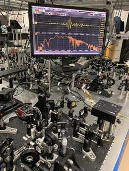
Image Caption: NIST’s tabletop frequency comb apparatus (foreground) can quickly identify molecules based on their absorption of infrared light. The yellow squiggle at the top of the screen is the electric field of mid-infrared laser light that has passed through air in the lab. The orange pattern at the bottom of the screen shows the corresponding spectrum of the light, with the downward spikes indicating the exact colors absorbed by water detected in the air.
The NIST setup, which occupies just a few square feet of table space, has potential applications such as disease diagnosis, identification of chemicals used in manufacturing, and biomass energy harvesting. The work is described in Science Advances.
Optical frequency combs measure exact frequencies, or colors, of light. Various comb designs have enabled the development of next-generation atomic clocks and show promise for environmental applications such as detecting methane leaks. Biological applications have been slower to develop, in part because it’s been hard to directly generate and measure the relevant infrared light.
To showcase biological applications, the NIST team used the new apparatus to detect “fingerprints” of NIST’s monoclonal antibody reference material, a protein made of more than 20,000 atoms that is used by the biopharmaceutical industry to ensure the quality of treatments.
“For the first time our frequency combs have simultaneous coverage across the entire infrared molecular fingerprint region,” project leader Scott Diddams said. “Other key advantages are speed, resolution and dynamic range in acquiring data.”
Mid-infrared light is an especially useful research probe because molecules usually rotate and vibrate at these frequencies. But until now it’s been difficult to probe this region due to a lack of broadband or tunable light sources and efficient detectors such as those available for visible and near-infrared light, the part of the infrared spectrum closest to visible light.
The new NIST apparatus overcomes these problems. Simple fiber lasers generate light spanning the entire range used to identify molecules—that is, mid-infrared to far-infrared wavelengths of 3-27 micrometers (frequencies of approximately 10-100 terahertz). The amounts of light absorbed at specific frequencies provide a unique signature of a molecule. The new system is innovative in detecting the electric fields of the absorbed light using photodiodes (light detectors) operating in the near-infrared range.
“A unique feature is that we detect signals in real time by rapidly sampling the infrared electric field with a near-infrared laser,” Diddams explained. “This has two advantages: It shifts the detection from the infrared to the near-infrared where we can use inexpensive telecommunications photodiodes, and we no longer suffer from the limitations of infrared detectors, which require cryogenic (liquid nitrogen) cooling.”
The researchers detected signature vibrations of three bands of amides (chemical groups containing carbon, oxygen, nitrogen and hydrogen) in the monoclonal antibody reference material. Amide bands in proteins are used to determine the folding, unfolding and aggregating mechanisms. Specific features of the detected bands indicated that the protein has a sheet structure, agreeing with previous studies. Sheets connect chemical groups in a flat arrangement.
In addition to biological applications, the new apparatus might be used to detect interactions between infrared light and condensed matter for quantum computing approaches that store data in molecular vibrations or rotations. In addition, when combined with novel imaging techniques, the tabletop system could obtain nanometer-scale images of samples that currently require the use of a much larger synchrotron facility.
Share on:


Subscribe
Stay ahead of the technologies shaping the future of electronics with our latest newsletter, Advanced Electronics Packaging Digest. Get expert insights on advanced packaging, materials, and system-level innovation, delivered straight to your inbox.
Subscribe now to stay informed, competitive, and connected.
Suggested Items
Gregoire Outters Promoted to President of Teledyne Marine Group
04/06/2026 | TeledyneTeledyne Technologies Incorporated announced the promotion of Gregoire Outters to President of its Teledyne Marine Group.
Teledyne Strengthens Commitment to the Space Sector
04/01/2026 | BUSINESS WIRETeledyne Technologies Incorporated is excited to announce the integration of the company’s extensive portfolio of space-focused technologies and businesses, reinforcing its long-term commitment to the global space sector.
Teledyne to Supply Detectors for Lazuli Space Observatory
03/30/2026 | BUSINESS WIRETeledyne Space Imaging, part of Teledyne Technologies Incorporated has been awarded a contract by Schmidt Sciences to deliver advanced near-infrared (NIR) H4RG-10 flight focal plane arrays (FPAs) and custom electronics for integration into the Integral Field Spectrograph on the groundbreaking Lazuli Space Observatory.
New Superconducting Chip Could Enable Breakthrough Nondestructive Terahertz Imaging
03/23/2026 | University of GlasgowA tiny crystal chip which uses terahertz radiation to see clearly through a wide range of materials could find applications in healthcare, biological research, and security screening.
The Test Connection Adds Creative Electron Prime TruVision™ X-ray and CT System for Deeper Failure Analysis
03/05/2026 | TTCIThe Test Connection Inc. (TTCI), a trusted provider of electronic test and manufacturing solutions for more than 45 years, has added the Prime TruVision™ X-ray and computed tomography (CT) inspection system from Creative Electron to its engineering and analysis services.