


 Driving Innovation: Mechanical and Optical Processes During Rigid-flex Production
 It’s Only Common Sense: Your Biggest Competitor Is Complacency
 The Chemical Connection: Onshoring PCB Production—Daunting but Certainly Possible


Building the Tools of the Next Manufacturing Revolution
June 18, 2019 | MITEstimated reading time: 6 minutes
Over a century ago, a visitor to Henry Ford’s new assembly line in Highland Park, Michigan, could watch workers build automobiles from interchangeable parts, and witness a manufacturing revolution in progress.
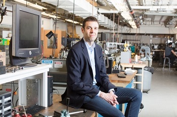
Today, someone who wants to glimpse the future of manufacturing should make a visit to John Hart’s lab. Through projects including next-generation 3-D printers, carbon nanotube fibers for use in electric motors and lightweight composites, and printing flexible materials for medical devices, Hart and his research group are developing technologies to reimagine the way things are made, from the nanoscale to the scale of the global economy.
Hart, an associate professor of mechanical engineering at MIT and the director of the Laboratory for Manufacturing and Productivity and the Center for Additive and Digital Advanced Production Technologies, is an expert in 3-D printing, also known as additive manufacturing, which involves the computer-guided deposition of material layer by layer into precise three-dimensional shapes. (Conventional manufacturing usually entails making a part by removing material, for example through machining, or by forming the part using a mold tool.)
Hart’s research includes the development of advanced materials — new types of polymers, nanocomposites, and metal alloys — and the development of novel machines and processes that use and shape materials, such as high-speed 3-D printing, roll-to-roll graphene growth, and manufacturing techniques for low-cost sensors and electronics.
“In my lab, through our partnerships with industry and via the startup companies I’m involved in, we’re seeking to redefine manufacturing at scale and rethink how resources are committed to manufacturing throughout the product life cycle,” Hart says. “One major focus is creating new kinds of 3-D printers. These are printers that are 10 to 100 times faster, more accurate, and process both well-known materials and materials that have never been possible before.”
A focus on applications and scale
Hart grew up in the Detroit area — one of the country’s great manufacturing hubs since Henry Ford’s time — and studied mechanical engineering as an undergraduate at the University of Michigan. He spent summers interning for General Motors, and when he started in the master’s degree program in mechanical engineering at MIT, he thought he would eventually make his way back to the auto industry.
Once he got to Cambridge, though, new horizons opened up. “Coming to MIT, I simply enjoyed the environment, the sense of challenge, learning, and open-mindedness,” he says.
Hart’s work with his advisor, professor of mechanical engineering Alexander Slocum, sparked an interest in nanomaterials manufacturing. He decided to pursue a PhD investigating new ways to build carbon nanotubes, which are long molecules that are stronger than steel and more conductive than copper.
When he returned to MIT in 2013 as a new faculty member, after several years as a professor at the University of Michigan, he started exploring another new frontier: 3-D printing.
As the director of the newly formed MIT Center for Additive and Digital Advanced Production Technologies and the co-founder of two Boston-area 3-D printing startups — Desktop Metal and VulcanForms — Hart is advancing this frontier on multiple fronts, through education, entrepreneurship, and engagement with industry.
Although the research projects in his lab span from the nanoscale to the macroscale, he has an eye trained on the bigger picture. Leveraging advances in computation, digitization, and automation, along with his own expertise with materials processing and machine design, Hart’s group sees the potential for 3-D printing to dramatically streamline and speed up global supply chains. The group is also pursuing a series of projects related to Hart’s longstanding interest in carbon nanotubes, exploring ways to form nanotubes into advanced wires, fibers, and structural composites.
Hart sees this convergence of digitally driven manufacturing technologies as a means of overcoming the logistical hurdles of long lead times, complex supply chains, and steep capital requirements.
And, he is motivated by finding new applications to benefit society at large. “That could be a better medical implant or sensor to measure the health of soil, a wire that is more conductive than copper, or a new business enabled by rapid access to 3-D printing in a dense city or a rural environment,” he says.
“If you want to make a new medical device, or even an automotive part, think of the supply chain you have to figure out and manage. Every part requires a lot of detail, time and investment to design, validate, and eventually produce, whether it’s made locally or overseas. One reason 3-D printing is fundamentally different is that it allows designers and engineers to iterate more quickly, and to, in the near future, produce parts on demand in large quantities without fixed up-front investment.”
Page 1 of 2
Share on:


Testimonial
"Advertising in PCB007 Magazine has been a great way to showcase our bare board testers to the right audience. The I-Connect007 team makes the process smooth and professional. We’re proud to be featured in such a trusted publication."
Klaus Koziol - atgSuggested Items
WestDev Announces Advanced Thermal Analysis Integration for Pulsonix PCB Design Suite
10/29/2025 | WestDev Ltd.Pulsonix, the industry-leading PCB design software from WestDev Ltd., announced a major enhancement to its design ecosystem: a direct interface between Pulsonix and ADAM Research's TRM (Thermal Risk Management) analysis software.
Designers Notebook: Power and Ground Distribution Basics
10/29/2025 | Vern Solberg -- Column: Designer's NotebookThe principal objectives to be established during the planning stage are to define the interrelationship between all component elements and confirm that there is sufficient surface area for placement, the space needed to ensure efficient circuit interconnect, and to accommodate adequate power and ground distribution.
Episode 6 of Ultra HDI Podcast Series Explores Copper-filled Microvias in Advanced PCB Design and Fabrication
10/15/2025 | I-Connect007I-Connect007 has released Episode 6 of its acclaimed On the Line with... American Standard Circuits: Ultra High Density Interconnect (UHDI) podcast series. In this episode, “Copper Filling of Vias,” host Nolan Johnson once again welcomes John Johnson, Director of Quality and Advanced Technology at American Standard Circuits, for a deep dive into the pros and cons of copper plating microvias—from both the fabricator’s and designer’s perspectives.
Nolan’s Notes: Tariffs, Technologies, and Optimization
10/01/2025 | Nolan Johnson -- Column: Nolan's NotesLast month, SMT007 Magazine spotlighted India, and boy, did we pick a good time to do so. Tariff and trade news involving India was breaking like a storm surge. The U.S. tariffs shifted India from one of the most favorable trade agreements to the least favorable. Electronics continue to be exempt for the time being, but lest you think that we’re free and clear because we manufacture electronics, steel and aluminum are specifically called out at the 50% tariff levels.
MacDermid Alpha & Graphic PLC Lead UK’s First Horizontal Electroless Copper Installation
09/30/2025 | MacDermid Alpha & Graphic PLCMacDermid Alpha Electronics Solutions, a leading supplier of integrated materials and chemistries to the electronics industry, is proud to support Graphic PLC, a Somacis company, with the installation of the first horizontal electroless copper metallization process in the UK.