


 Marcy’s Musings: Advancing the Advanced Materials Discussion
 The Marketing Minute: Cracking the Code of Technical Marketing
 Trouble in Your Tank: Implementing Direct Metallization in Advanced Substrate Packaging


Tuning the Energy Levels of Organic Semiconductors
July 5, 2019 | TU DresdenEstimated reading time: 2 minutes
Physicists from the Dresden Integrated Center for Applied Physics and Photonic Materials (IAPP) and the Center for Advancing Electronics Dresden (cfaed) at the TU Dresden, together with researchers from Tübingen, Potsdam and Mainz were able to demonstrate how electronic energies in organic semiconductor films can be tuned by electrostatic forces. A diverse set of experiments supported by simulations were able to rationalize the effect of specific electrostatic forces exerted by the molecular building blocks on charge carriers.
In electronic devices based on organic semiconductors such as solar cells, light-emitting diodes, photodetectors or transistors, electronic excitations and charge transport levels are important concepts to describe their operation principles and performances. The corresponding energetics, however, are more difficult to access and to tune than in conventional inorganic semiconductors like silicon chips, which stands as a general challenge. This applies both to the measurement and to the controlled influence from outside.
One tuning knob exploits the long-range Coulomb interactions, which is enhanced in organic materials. In the present study, the dependence of the energies of charge transport levels and of excitonic states on blend composition and molecular orientation in the organic material is explored. Excitons are bound pairs of an electron and a hole that are formed in the semiconductor material by light absorption. Scientists refer to blend composition when the components consist of different organic semiconducting materials. The findings demonstrate that the energetics in organic films can be tuned by adjusting a single molecular parameter, namely the molecular quadrupole moment in the pi-stacking direction of the molecules. An electric quadrupole can consist of two positive and two equally strong negative charges which form two oppositely equal dipoles. In the simplest case, the four charges are alternately arranged at the corners of a square.
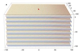
Examples of film structures used for the calculations of the charge—quadrupole interaction energy (EQ) of crystalline films in edge-on (a) and face-on orientation (b). The molecules are represented by discs for illustration purpose. The length scale is given in Å. EQ values are calculated for the red molecules at the film surface.
The authors further link device parameters of organic solar cells such as the photovoltage or the photocurrent to this quadrupole moment. The results help to explain recent breakthroughs of device efficiency in organic solar cells, which are based on a new class of organic materials. As the observed electrostatic effect is a general property of organic materials, including so-called “small molecules” and polymers, it can help to improve the performance of all types of organic devices.
Share on:


Testimonial
"We’re proud to call I-Connect007 a trusted partner. Their innovative approach and industry insight made our podcast collaboration a success by connecting us with the right audience and delivering real results."
Julia McCaffrey - NCAB GroupSuggested Items
Curing and Verification in PCB Shadow Areas
09/17/2025 | Doug Katze, DymaxDesign engineers know a simple truth that often complicates electronics manufacturing: Light doesn’t go around corners. In densely populated PCBs, adhesives and coatings often fail to fully cure in shadowed regions created by tall ICs, connectors, relays, and tight housings.
Marcy’s Musings: Advancing the Advanced Materials Discussion
09/17/2025 | Marcy LaRont -- Column: Marcy's MusingsAs the industry’s most trusted global source of original content about the electronics supply chain, we continually ask you about your concerns, what you care about, and what you most want to learn about. Your responses are insightful and valuable. Thank you for caring enough to provide useful feedback and engage in dialogue.
September 2025 PCB007 Magazine: The Future of Advanced Materials
09/16/2025 | I-Connect007 Editorial TeamMoore’s Law is no more, and the advanced material solutions being developed to grapple with this reality are surprising, stunning, and perhaps a bit daunting. Buckle up for a dive into advanced materials and a glimpse into the next chapters of electronics manufacturing.
I-Connect007 Launches Advanced Electronics Packaging Digest
09/15/2025 | I-Connect007I-Connect007 is pleased to announce the launch of Advanced Electronics Packaging Digest (AEPD), a new monthly digital newsletter dedicated to one of the most critical and rapidly evolving areas of electronics manufacturing: advanced packaging at the interconnect level.
Panasonic Industry will Double the Production Capacity of MEGTRON Multi-layer Circuit Board Materials Over the Next Five Years
09/15/2025 | Panasonic Industry Co., Ltd.Panasonic Industry Co., Ltd., a Panasonic Group company, announced plans for a major expansion of its global production capacity for MEGTRON multi-layer circuit board materials today. The company plans to double its production over the next five years to meet growing demand in the AI server and ICT infrastructure markets.