-

- News
- Books
Featured Books
- smt007 Magazine
Latest Issues
Current Issue
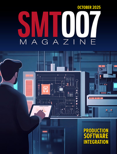
Production Software Integration
EMS companies need advanced software systems to thrive and compete. But these systems require significant effort to integrate and deploy. What is the reality, and how can we make it easier for everyone?

Spotlight on India
We invite you on a virtual tour of India’s thriving ecosystem, guided by the Global Electronics Association’s India office staff, who share their insights into the region’s growth and opportunities.

Supply Chain Strategies
A successful brand is built on strong customer relationships—anchored by a well-orchestrated supply chain at its core. This month, we look at how managing your supply chain directly influences customer perception.
- Articles
- Columns
- Links
- Media kit
||| MENU - smt007 Magazine
The Jefferson Institute of Technology: Facts and Updates
July 5, 2019 | The Jefferson ProjectEstimated reading time: 2 minutes
Founded by Tom Borkes, the Jefferson Project—through the Jefferson Institute of Technology (JIT)—aims to build and maintain a world class workforce for the domestic electronics manufacturing industry, while showcasing state-of-the-art equipment and developing emerging assembly technologies.
Based on the principles of Concurrent Education, JIT will use a state-of-the-art not-for-profit business—the Jefferson Electronic Manufacturing Center (JEM Center)—as the environment for learning during the entire tenure of a student's education. Students will receive an intensive, continually updated academic program, using the manufacturing business as their classroom. Hands-on experience in every facet of the manufacturing operation will teach real-world skills and problem solving. In addition, product developers and equipment manufacturers can observe the latest electronic packaging technologies in a real-world application.
Here are some JIT facts:
1. JIT will be co-located with the JEM Center, a contract manufacturing (EMS) business.
2. The JEM Center will provide the student with a real-world classroom to supplement the traditional undergraduate engineering education.
3. Over four years, JIT students will participate in every aspect of the JEM Center operation—and, be paid for their contributions.
4. Successful completion of the four-year JIT program will result in a B.S. in Applied Product Design and Production Sciences.
5. Each product assembly process step continues to be scrutinized and assigned to a traditional applicable engineering class, e.g., printing solder paste to chemistry, fluid dynamics, etc. The JIT class is then supplemented with process-related content.
6. The JIT academic year will consist of three, 16-week trimesters.
7. Students will graduate with APICS (Material & Supply Chain Management) and ASQ (Including 6-Sigma Black Belt) certifications. They also will have taken the Fundamentals in Engineering (FE) Exam that can lead to a P.E license.
8. Real world issues encountered by the student in the JEM Center operation will be addressed in real time. These issues, many without closed-form solutions, will permit the student to develop a crucial skill: good judgment—invaluable to their future employers.
9. Corporate sponsors will provide leading edge automation equipment and supplies. Students will always be learning in a state-of-the art environment.
10. Basic student tuition is $5,000/trimester. Corporate student sponsorships, scholarships and the paid work in the JEM Center can reduce this cost.
11. Curriculum development is partially based on Mortimer Adler’s Paideia Proposal and The Great Books, but with a blending of Learning for Learning, AND Learning for Earning.
12. The School’s development borrows from the Jeffersonian strategy he used for The University of Virginia.
13. Formal contracts between students and JEM’s clients will guarantee students a job upon graduation, and guarantee the client companies employees with a world class education—those educated by building the company’s products.
A freshman, Trimester 1 class listing has already been released, where “Civics” and “Organizational & Personal Ethics in an Engineering Environment” classes have been added. For more information, contact Tom Borkes at jeffer2@earthlink.net.
Testimonial
"We’re proud to call I-Connect007 a trusted partner. Their innovative approach and industry insight made our podcast collaboration a success by connecting us with the right audience and delivering real results."
Julia McCaffrey - NCAB GroupSuggested Items
Rehm Wins Mexico Technology Award for CondensoXLine with Formic Acid
10/17/2025 | Rehm Thermal SystemsModern electronics manufacturing requires technologies with high reliability. By using formic acid in convection, condensation, and contact soldering, Rehm Thermal Systems’ equipment ensures reliable, void-free solder joints — even when using flux-free solder pastes.
Indium Experts to Deliver Technical Presentations at SMTA International
10/14/2025 | Indium CorporationAs one of the leading materials providers to the power electronics assembly industry, Indium Corporation experts will share their technical insight on a wide range of innovative solder solutions at SMTA International (SMTAI), to be held October 19-23 in Rosemont, Illinois.
Knocking Down the Bone Pile: Revamp Your Components with BGA Reballing
10/14/2025 | Nash Bell -- Column: Knocking Down the Bone PileBall grid array (BGA) components evolved from pin grid array (PGA) devices, carrying over many of the same electrical benefits while introducing a more compact and efficient interconnect format. Instead of discrete leads, BGAs rely on solder balls on the underside of the package to connect to the PCB. In some advanced designs, solder balls are on both the PCB and the BGA package. In stacked configurations, such as package-on-package (PoP), these solder balls also interconnect multiple packages, enabling higher functionality in a smaller footprint.
Indium to Showcase High-Reliability Solder and Flux-Cored Wire Solutions at SMTA International
10/09/2025 | Indium CorporationAs one of the leading materials providers in the electronics industry, Indium Corporation® will feature its innovative, high-reliability solder and flux-cored wire products at SMTA International (SMTAI), to be held October 19-23 in Rosemont, Illinois.
‘Create your Connections’ – Rehm at productronica 2025 in Munich
10/08/2025 | Rehm Thermal SystemsThe electronics industry is undergoing dynamic transformation: smart production lines, sustainability, artificial intelligence, and sensor technologies dominate current discussions.


