


 Dan’s Biz Bookshelf: ‘Abundance: How We Build a Better Future’
 Trouble in Your Tank: In Complex Systems, Design Rules Aren’t Optional
 It’s Only Common Sense: The Phone Is Still Your Competitive Advantage


Terahertz Technology Escapes the Cold
July 10, 2019 | ETH ZurichEstimated reading time: 4 minutes
Terahertz (THz) radiation is a bit like a treasure chest that resists being opened fully. Residing in the electromagnetic spectrum between the infrared and microwave regions, THz radiation combines a range of properties that are ideal with a view to applications. It provides a window to unique spectroscopic information about molecules and solids, it can penetrate non-conducting materials such as textiles and biological tissue, and it does so without ionising—and hence damaging—the object, or subject, under study. This opens up intriguing prospects for non-invasive imaging and non-destructive quality control, among other applications. But whereas there is no shortage in ideas for potential uses, their implementation is hampered by a lack of practical technologies for generating and detecting THz radiation.
Therefore the excitement as Lorenzo Bosco, Martin Franckié and colleagues from the group of Jérôme Faist at the Institute for Quantum Electronics of ETH Zurich reported now the realization of a THz quantum cascade laser that operates at a temperature of 210 K (-63 °C). That is the highest operational temperature achieved so far for this type of device. More importantly, this is the first time that operation of such a device has been demonstrated in a temperature regime where no cryogenic coolants are needed. Instead, Bosco et al. used a thermoelectric cooler, which is much more compact, cheaper and easier to maintain than cryogenic equipment. With this advance, they removed the main obstacles on the route to various practical applications.
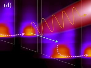
a) The thermoelectrically cooled laser box with the laser mounted on top of a Peltier element (white square), allowing operation between 195 K and 210.5 K with the laser emitting vertically through the window in the top lid. b) The laser chip as mounted in the laser box, contacted with thin gold wires bonded on top of several laser ridges. c) Schematic of one laser ridge; the horizontal lines show the quantum-well structure formed by layered semiconductors. The ridge (150 micrometres wide) is sandwiched between thin layers of copper. d) Conduction band edge (white lines) tilted by the applied operation bias, with the electron density resolved in energy shown in colour. The electrical bias drives electrons through the non-radiative transitions indicated by the dashed arrow. This pumps the state in the thin well, which becomes more populated than the state in the wider well indicated by the green arrow, allowing for net stimulated emission of terahertz photons.
A Cascade Towards Applications
Quantum cascade lasers (QCLs) have long been established as a natural concept for THz devices. Like many lasers that are widely used as sources of light in the visible-to-infrared frequency region, QCLs are based on semiconductor materials. But compared to typical semiconductor lasers used, for instance, in barcode readers or laser pointers, QCLs operate according to a fundamentally different concept to achieve light emission. In short, they are built around repeated stacks of precisely engineered semiconductor structures (see the figure, panel c), which are designed such that suitable electronic transitions take place in them (panel d). QCLs have been proposed in 1971, but they were first demonstrated only in 1994, by Faist and colleagues, then working at Bell Laboratories (US). The approach has proved its value in a board range of experiments, both fundamental and applied, mainly in the infrared region. The development of QCLs for THz emission has made substantial advances, too, starting from 2001. Widespread use has been hindered though by the requirement for cryogenic coolants -- typically liquid helium -- which adds substantial complexity and cost, and makes devices large and less mobile. Progress towards operation of THz QCLs at higher temperatures got essentially stuck seven years ago, when operation of devices at around 200 K (-73 °C) was achieved.
Page 1 of 2
Share on:


Subscribe
Stay ahead of the technologies shaping the future of electronics with our latest newsletter, Advanced Electronics Packaging Digest. Get expert insights on advanced packaging, materials, and system-level innovation, delivered straight to your inbox.
Subscribe now to stay informed, competitive, and connected.
Suggested Items
Driving Innovation: Selecting the Right Laser Source
04/28/2026 | Simon Khesin -- Column: Driving InnovationWhen I first joined Schmoll Maschinen, I brought experience from almost every PCB process, except for laser. As I immersed myself in laser processing, I realized why it can seem so daunting to a newcomer. The complexity arises from three intersecting factors: A vast variety of laser sources: CO2, UV-nano, green-pico, UV-pico, IR-pico, and others; a diverse range of applications: Drilling, cutting, ablation, and more; and an extensive list of materials: These have vastly different absorption rates. Choosing the right machine or laser source is rarely trivial. Even for experienced engineers, answering "Which source is best?" requires examining the business's specific goals.
Institute of Circuit Technology Spring Seminar 2026: A Bright Future in Europe
04/23/2026 | Pete Starkey, I-Connect007Through the leafy lanes and spring flowers of Warwickshire and back to Meridan, the traditional centre of England, and now officially part of the Metropolitan Borough of Solihull in the county of the West Midlands, I attended the Annual General Meeting and Spring Seminar of the Institute of Circuit Technology (ICT) on April 14. Out of the AGM came notable changes in leadership at the top of the Institute: the retirement of Mat Beadel as chair and Emma Hudson as technical director. Effective May 1, Steve Driver is the new chair, and Alun Morgan is the new technical director.
ACCM Unveils Negative and Near-zero CTE Materials for Large-Format AI Chips
04/21/2026 | Advanced Chip and Circuit MaterialsAdvanced Chip and Circuit Materials, Inc. (ACCM) has launched two new materials: Celeritas HM50, with a negative coefficient of thermal expansion (CTE) of -8 ppm/°C to offset the positive CTE and expansion of copper with temperature on circuit boards, and Celeritas HM001, with near-zero CTE and the low-loss performance needed for high-speed signal layers to 224 Gb/s and faster in artificial intelligence (AI) circuits.
Fresh PCB Concepts: Designing PCBs for Harsh Environments—Reliability Is Engineered Upstream
04/23/2026 | Team NCAB -- Column: Fresh PCB ConceptsWhen engineers hear the phrase “harsh environment,” they usually think of the extreme temperature swings, vibration and shock, pressure changes, or radiation in aerospace. However, aerospace is not the only harsh environment where electronic assemblies must survive. Automotive power electronics, downhole oil and gas tools, marine controls, rail systems, defense platforms, and industrial automation equipment all expose PCBs to environments that are equally unforgiving. The stress mechanisms may differ, but the physics does not.
Advanced Packaging for AI: Reliability Starts at the Cu/Cu/Cu Microvia Junction
04/20/2026 | Kuldip Johal, MKS' AtotechThe rapid growth of AI computing, from training clusters to inference at scale, is reshaping demand across the entire electronics supply chain. Advances in technology requirements, such as higher bandwidth, lower latency, and greater compute density, are driving the development of advanced packaging technologies and transforming the PCB industry across design, manufacturing, testing, and even architecture.