


 Dan’s Biz Bookshelf: ‘Abundance: How We Build a Better Future’
 Trouble in Your Tank: In Complex Systems, Design Rules Aren’t Optional
 It’s Only Common Sense: The Phone Is Still Your Competitive Advantage


Microrobots to Change the Way We Work With Cellular Material
July 12, 2019 | University of TorontoEstimated reading time: 2 minutes
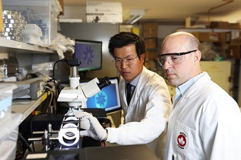
In a new study published in the Proceedings of the National Academy of Sciences, researchers in the lab of Professor Aaron Wheeler (Chemistry, IBBME) have demonstrated a novel and non-invasive way to manipulate cells through microrobotics.
Cell manipulation — which requires moving small particles from one place to another — is an integral part of many scientific endeavours. One method of manipulating cells is through optoelectronic tweezers (OET), which use various light patterns to directly interact with the object of interest.
Because of this direct interaction, there are limitations to the force that can be applied and speed in which the cellular material can be manipulated. This is where the use of microrobotics becomes useful.
Led by postdoctoral fellow Dr. Shuailong Zhang (Chemistry) and Wheeler, the researchers have designed microrobots (working at the sub-millimetre scale) that can be operated by OET for cell manipulation.
Instead of using light to directly interact with the cells, the light is used to steer cogwheel-shaped microrobots that can “scoop up” cell material, transport it and then deliver it. This manipulation can be done at greater speeds while causing less damage to the material compared to traditional OET methods.
“The ability of these light-driven microrobots to perform non-invasive and accurate control, isolation and analysis of cells in complex biological environment make them a very powerful tool,” says Zhang.
“Traditional techniques that are used to manipulate single cells while evaluating them by microscopy is slow and tedious, requiring a lot of expertise to carry out,” says Wheeler, who is also cross-appointed to the Donnelly Centre for Cellular and Biomolecular Research.
“But these microrobots are inexpensive and very simple to use and they have a wide range of applications in the life sciences and beyond.”
In addition to cell analysis, the microrobots can also be used in cell sorting (for clonal expansion), RNA sequencing and cell-cell fusion (commonly used in the production of antibodies).
“Neural stem cells are responsive to a multitude of cues and environmental stimuli in their niche, and these change with injury, so teasing out the signals, and cell responses, is a huge challenge when we are trying to harness the potential of stem cells for neural repair,” says Professor Cindi Morshead(IBBME, Surgery), who is a co-author of the study. Her research in regenerative medicine works with neural stem cells that reside in the brain and spinal cord.
“These microrobots allow for the exquisite control of the cells and their microenvironment, tools that we will need to learn how best to activate the stem cells.”
Share on:


Subscribe
Stay ahead of the technologies shaping the future of electronics with our latest newsletter, Advanced Electronics Packaging Digest. Get expert insights on advanced packaging, materials, and system-level innovation, delivered straight to your inbox.
Subscribe now to stay informed, competitive, and connected.
Suggested Items
SMTA Ultra HDI Symposium, Day 1: AI at the Core or Out of the Game
04/13/2026 | Marcy LaRont, I-Connect007It was a beautiful 81°F morning in Arizona last Wednesday as I headed to the third annual SMTA Ultra HDI Symposium, focused on AI and ultra high density interconnect technology. Strategically held as part of Arizona’s Tech Week, this year’s conference took place in Avondale in Phoenix's West Valley. The event moved from the cozy offices of the Peoria Sports Complex (which paid homage to baseball’s spring training world) to the larger Avondale Conference Center, highlighting the importance of this area for electronics manufacturing investment.
PCBAA Sets Its Priorities for 2026: Support in the House and Senate
02/03/2026 | Marcy LaRont, I-Connect007David Schild, executive director of the Printed Circuit Board Association of America (PCBAA), leads an organization focused on the domestic manufacture of PCBs and substrates to support America’s critical microelectronics supply. In the continuation of this interview, David talks about the ways his organization is aligning its priorities with Washington, in particular, the Executive Branch. It might feel like a snail’s pace, but progress could mean financial support and more domestic security, even for the smaller companies.
SMT Perspectives & Prospects: Artificial Intelligence Part 6: Data Module 1
10/07/2025 | Dr. Jennie Hwang -- Column: SMT Perspectives and ProspectsData is one of the six pillars of AI infrastructure. It is critical to the performance of artificial intelligence (AI) models. AI data, essential to both the training and inference of Generative AI models, connotes the datasets used to train, validate, and test AI models. Training data provides models with a frame of reference by establishing a baseline against which models can compare new data using pre-trained models for predictions or generating new content.
U.S. Uses Secret Trackers to Trace AI Chips Diverted to China, Sources Say
08/18/2025 | I-Connect007 Editorial TeamTwo sources told Reuters that U.S. authorities have secretly placed location trackers in some advanced chip shipments they see as at high risk of illegal diversion to China. They said the trackers are intended to locate AI chips that are sent to locations restricted by U.S. export laws, but authorities only examine some shipments.
Happy’s Tech Talk #38: Novel Metallization for UHDI
05/07/2025 | Happy Holden -- Column: Happy’s Tech TalkI have been involved in high-density electronics substrates since 1970 when I joined Hewlett-Packard’s RF semiconductor group after college. Figure 1 shows the difference between trace/space lithography for substrates and silicon starting in 1970. My projects involved sapphire circuits for RF devices, but the figure displays the state of PCBs and integrated CMOS circuits and their packaging, not discreet RF devices. Even then, semiconductors were 50X higher density.