


 Dan’s Biz Bookshelf: ‘Abundance: How We Build a Better Future’
 Trouble in Your Tank: In Complex Systems, Design Rules Aren’t Optional
 It’s Only Common Sense: The Phone Is Still Your Competitive Advantage


On the Way to Printable Organic Light Emitting Diodes
July 15, 2019 | Max Planck Institute for Polymer ResearchEstimated reading time: 2 minutes
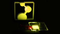
Organic light-emitting diodes are components that no longer consist of compounds containing the semiconducting material gallium, but of so-called organic compounds in which carbon is a main component. Compared to conventional light-emitting diodes, however, the luminosity and lifetime of OLEDs are currently lower, which is why they represent a current field of research.
Scientists at the MPI-P led by group leader Gert-Jan Wetzelaer (Department of Prof. Paul Blom) have now developed a new OLED concept. Nowadays, OLEDs consist of various wafer-thin layers. Some layers are used to transport charges, while others are used to efficiently introduce electrons into the active layer in which light is generated. Thus, current OLEDs can easily consist of five to seven layers. The researchers have now developed an OLED which consists only of one single layer that is supplied with electricity via two electrodes. This simplifies the production of such OLEDs and paves the way for printable displays.
With their first prototype, the Mainz scientists were able to show that they can generate a brightness of the emitted light of 10,000 candela/square meter with a voltage of only 2.9 volts - this corresponds to about 100 times the luminosity of modern screens. Achieving such high luminosity at this low voltage is a record for current OLEDs. The researchers were also able to measure an external efficiency of 19%, which means that 19% of the electrical energy supplied is converted into light that comes out in direction of the viewer. Also with this value, the OLED prototype can compete with current OLEDs consisting of five or even more layers.
In continuous operation, the researchers were able to measure a so-called LT50 lifetime of almost 2000 hours at a brightness equivalent to ten times that of modern displays. Within this time, the initial luminosity has dropped to 50% of its value.
"For the future, we hope to be able to improve the concept even further and thus achieve even longer lifetimes. This means that the concept could be used for industrial purposes," says Wetzelaer. The scientists hope that their newly developed single-layer concept - i.e. the reduced complexity of OLEDs - will contribute to the identification and improvement of the processes responsible for the reduction in luminance over time.
The scientists are using a light-emitting layer based on so-called “Thermally Activated Delayed Fluorescence” (TADF). This physical principle has been known for several decades, but became the focus of OLED research about 10 years ago, when an efficient conversion of electrical energy into light was demonstrated in Japan. Since then, researchers have been working to produce TADF-based OLEDs, as these do not require expensive molecular complexes containing rare-earth metals that are being used in current OLEDs.
Share on:


Subscribe
Stay ahead of the technologies shaping the future of electronics with our latest newsletter, Advanced Electronics Packaging Digest. Get expert insights on advanced packaging, materials, and system-level innovation, delivered straight to your inbox.
Subscribe now to stay informed, competitive, and connected.
Suggested Items
SMTA Ultra HDI Symposium, Day 1: AI at the Core or Out of the Game
04/13/2026 | Marcy LaRont, I-Connect007It was a beautiful 81°F morning in Arizona last Wednesday as I headed to the third annual SMTA Ultra HDI Symposium, focused on AI and ultra high density interconnect technology. Strategically held as part of Arizona’s Tech Week, this year’s conference took place in Avondale in Phoenix's West Valley. The event moved from the cozy offices of the Peoria Sports Complex (which paid homage to baseball’s spring training world) to the larger Avondale Conference Center, highlighting the importance of this area for electronics manufacturing investment.
PCBAA Sets Its Priorities for 2026: Support in the House and Senate
02/03/2026 | Marcy LaRont, I-Connect007David Schild, executive director of the Printed Circuit Board Association of America (PCBAA), leads an organization focused on the domestic manufacture of PCBs and substrates to support America’s critical microelectronics supply. In the continuation of this interview, David talks about the ways his organization is aligning its priorities with Washington, in particular, the Executive Branch. It might feel like a snail’s pace, but progress could mean financial support and more domestic security, even for the smaller companies.
SMT Perspectives & Prospects: Artificial Intelligence Part 6: Data Module 1
10/07/2025 | Dr. Jennie Hwang -- Column: SMT Perspectives and ProspectsData is one of the six pillars of AI infrastructure. It is critical to the performance of artificial intelligence (AI) models. AI data, essential to both the training and inference of Generative AI models, connotes the datasets used to train, validate, and test AI models. Training data provides models with a frame of reference by establishing a baseline against which models can compare new data using pre-trained models for predictions or generating new content.
U.S. Uses Secret Trackers to Trace AI Chips Diverted to China, Sources Say
08/18/2025 | I-Connect007 Editorial TeamTwo sources told Reuters that U.S. authorities have secretly placed location trackers in some advanced chip shipments they see as at high risk of illegal diversion to China. They said the trackers are intended to locate AI chips that are sent to locations restricted by U.S. export laws, but authorities only examine some shipments.
Happy’s Tech Talk #38: Novel Metallization for UHDI
05/07/2025 | Happy Holden -- Column: Happy’s Tech TalkI have been involved in high-density electronics substrates since 1970 when I joined Hewlett-Packard’s RF semiconductor group after college. Figure 1 shows the difference between trace/space lithography for substrates and silicon starting in 1970. My projects involved sapphire circuits for RF devices, but the figure displays the state of PCBs and integrated CMOS circuits and their packaging, not discreet RF devices. Even then, semiconductors were 50X higher density.