


 Learning with Leo: Drones—Meeting Demand Without Compromise
 Nolan’s Notes: Our Spotlight on North America
 Global Sourcing Spotlight: Building a Supply Chain That Bends, Not Breaks


Practical Implementation of Assembly Processes for Low Melting Point Solder Pastes (Part 1)
July 16, 2019 | Adam Murling, Miloš Lazić, and Don Wood, Indium Corporation; and Martin Anselm, Rochester Institute of TechnologyEstimated reading time: 5 minutes
Bismuth-tin solder alloys have drawn interest for electronics applications for decades. The melting point around 140°C is very desirable because it allows for the use of lower temperature laminate materials and reduces thermal stress on sensitive components. Originally, it was considered a good alternative to wave soldering processes bolstered by the intrinsic reliability of through-hole components.
Since 2006 and the implementation of the RoHS directive, the interest in bismuth-tin solder alloys has only increased as the industry has searched for Pb-free alternatives to the chosen standard, SAC305, which melts at considerably higher temperatures than the incumbent tin-lead alloys.
Now, there are new drivers toward consideration of low melting point alloys. Lower processing temperatures are tempting because they reduce process costs. Lower processing temperatures may also facilitate designs that would be challenging to assemble with tin-based alloys. Additionally, as component architectures get thinner, component manufacturers have explored the option to align the solder alloy melting point with the inflection point where component warpage is at its least.
These factors have driven renewed interest in bismuth-tin alloys and the development of new alloy options with improved mechanical properties. These new alloys options also include alloys composed of tin and indium, or bismuth-tin with minor elemental additions of silver, antimony, or nickel.
This two-part article will discuss the background and need for low-temperature solders and compare the “processability” of solder pastes with three novel alloys against the industry standard 57Bi/42Sn/1Ag.
Background
The most noticeable difference in the performance of bismuth-tin alloys is the brittleness of the resulting solder joints. This eliminates bismuth-tin as an option for applications where drop shock reliability is critical. Other properties, such as thermal cycling reliability and electrical/thermal performance, are promising. Further alloy development has been focused on maximizing these forms of reliability, resulting in more robust low melting point soldering solutions.
Regarding thermal cycling, bismuth-tin alloys have a shorter life due to peak cycling temperatures in closer proximity to the lower melting point. This increases the challenge associated with such testing. When you couple this with a less-than-optimal thermal conductivity rating, solder joint failure becomes a major concern for reliability, especially for high-current applications.
Early adopters of bismuth-tin alloys had to be very careful about interaction with lead (Pb). If the alloy made contact with any amount of lead, such as on component leads or board surface finishes, a phase was formed that melts at a much lower temperature and compromises the integrity of solder joints [1].
Reliability studies have shown that silver additions as little as 1% substantially increase thermal conductivity, shear strength, and tensile strength while still providing a low melting point alternative to Pb-based alloys. With 1% silver, the resulting melting point is 138–140°C. Most early applications adopted this alloy because of the considerable benefits without tradeoffs.
Careful consideration must be used when choosing a flux vehicle for low melting point solder pastes. The flux that is chosen must activate at a much lower temperature than standard fluxes due to the low melting point. A majority of fluxes used in 63Sn/37Pb or SAC305 are not recommended for low melting point alloys. To increase the reliability of the alloy and ensure a robust solder joint, the flux vehicle is imperative.
As technology advances, the performance requirements for low-temperature alternatives are becoming more demanding. Solder pastes developed in the early adoption of the bismuth-tin eutectic alloy do not achieve printing and reflow performances to rival modern Pb-free solder pastes. Recent studies [2] have focused on the reliability of newly developed alloys but have overlooked the “process-ability” in solder paste form. Bulk properties of an alloy may be promising, but if a solder paste does not have excellent stencil printing, stability, and reflow performance, it will not be easily adopted.
Experiment
In this experiment, four solder pastes were printed and tested: a bismuth-containing baseline (57Bi/42Sn/1Ag), two novel bismuth-based alloys, and an indium-based alloy.
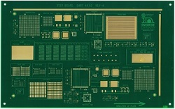
All solder pastes used were brought to room temperature before stencil printing. Common, commercially available equipment was used for test board preparation. Stencil printing used a 120-µm laser-cut and electro-polished stencil with a nano-coating. The test board design (Figure 1) included print-to-fail patterns with challenging area ratios as well as areas for component placement. ENIG finish test boards were used for setup.
Figure 1: Test vehicle.
Print Quality Results
The printing procedure was designed to test solder pastes’ resilience to a pause mechanism. In this test, there was one one-hour pause presented after printing 12 PCBs, performing an under-stencil wipe, and then progressing with printing an additional 12 PCBs. The test vehicle is pictured in Figure 1. All of the volumetric data for the print quality section was analyzed using JMP® Statistical Software from SAS. That same data was then separated using the variability/attribute gauge chart function by the following characteristics:
- Alloy selection
- Aperture size
- Aperture shape
- Mask characteristics
To compare the five different lots across all of the different variables, a spreadsheet containing 21,901,152 cells of data was created. To separate the data efficiently, a naming convention was used for each pad combination. A string of characters was created with the first three letters being either print-to-fail (PTF) or chip (CHP) followed by the size of the aperture in microns, a C or an M—which denotes whether the pad is either copper defined* or mask defined—and finally, the shape of the pad (square or circle).
*The boards are denoted as copper defined even if the board metallization is another metal. In this test, the ENIG boards were not reflowed. This decision was based on trying to avoid confusion and promoting consistency within the naming convention.
The printing and solder paste variables, along with the board number and paste type, are displayed on the X-axis in the variability chart while the volume percent is positioned on the Y-axis. The complete data set is structured by each aperture size in the following order:
- 220-micron copper/mask defined circles and squares
- 230-micron copper/mask defined circles and squares
- 240-micron copper/mask defined circles and squares
- 260-micron copper/mask defined circles and squares
- 280-micron copper/mask defined circles and squares
- 300-micron copper/mask defined circles and squares
- 0201 chip pads 320x230-micron copper defined
- 0402 chip pads 900x700-micron copper defined
The following variability charts show all of the above aperture sizes with copper (metal) defined, circles and the 0201 and 0402 pads. The data displayed in Figures 2–7 show comparison results of the different alloyed solder pastes. It is important to note that the data was taken using a 120-µm nano-coated stencil. The printing parameters were all kept constant.
Figure 2: 300-μm copper defined circle variability chart.
Figure 3: 300-μm copper defined circle standard deviation chart.
Figure 4: 0201 320x230-μm copper defined variability chart.
Figure 5: 0201 320x230-μm copper defined standard deviation chart.
Figure 6: 0402 900x700-μm copper defined variability chart.
Figure 7: 0402 900x700-μm copper defined standard deviation.
The printing performance across the alloys is consistent with what would be expected of the area ratios for this stencil thickness. It was interesting to view how the indium-containing alloy seemed to experience more variation across the various aperture sizes compared to the bismuth equivalent. This may indicate that the flux chosen was not an ideal match.
The two novel bismuth alloys printed similarly to the baseline 57Bi/42Sn/1Ag alloy. There was an expectation that the solder pastes response-to-pause performance would be concerning. However, considering the aperture size and area ratios, they printed relatively well, especially as the apertures grew in size.
Stay tuned for Part 2 of this experiment, including reflow results and conclusions.
Acknowledgments
- David Sbiroli, technical manager, global accounts, Indium Corporation
- Eric Bastow, assistant technical manager, America’s region, Indium Corporation
- Meagan Sloan, technical support engineer, Indium Corporation
- Rochester Institute of Technology
References
- E. Ferrer and H. Holder, “57Bi-42Sn-1Ag: A Lead-Free, Low-Temperature Solder for the Electronic Industry,” IPC JEDEC 4th International Conference on Lead-Free Electronic Components and Assemblies, 2003.
- H. Fu, R. Aspandiar, J. Chen, S. Cheng, Q. Chen, R. Coyle, S. Feng, M. Krmpotich, R.C. Lasky, S. Mokler, J. Radhakrishnan, M. Ribas, B. Sandy-Smith11, K.K. Tang, G. Wu, A. Zhang, and W. Zhen, “iNEMI Project on Process Development of BiSn-Based Low-Temperature Solder Pastes,” SMTAi 2017.
This paper was first presented at SMTAi 2018 and published in the technical proceedings.
Share on:


Testimonial
"We’re proud to call I-Connect007 a trusted partner. Their innovative approach and industry insight made our podcast collaboration a success by connecting us with the right audience and delivering real results."
Julia McCaffrey - NCAB GroupSuggested Items
AQUANOX A4727 and A4625 Lead KYZEN Offerings at SMTA Oregon Expo and Tech Forum
05/06/2026 | KYZENKYZEN, the global leader in innovative environmentally responsible cleaning chemistries, will exhibit at the SMTA Oregon Expo and Tech Forum scheduled to take place Thursday, May 19 at the Wingspan Event and Conference Center in Hillsboro, Oregon.
Connect the Dots: Designing for the Future of Manufacturing Reality—Surface Finish
05/07/2026 | Matt Stevenson -- Column: Connect the DotsWhen designing the complex boards that many electronic devices require to operate, designers should consider manufacturability at every step. This is my last article focused on designing for the always-evolving manufacturing reality. Choosing the right surface finish has always been important. If you are creating intricate designs with a wide variety of components, like for an ultra-high density interconnect (UHDI) board, surface finish is a critical last step.
Indium to Showcase High-Performance AI Application Solutions at SEMICON SEA 2026
05/01/2026 | Indium CorporationAs a leading provider of advanced materials solutions for today’s demanding AI applications, Indium Corporation® will feature its high-reliability product portfolio at SEMICON SEA 2026, May 5-7, in Kuala Lumpur, Malaysia.
ACCM Unveils Negative and Near-zero CTE Materials for Large-Format AI Chips
04/21/2026 | Advanced Chip and Circuit MaterialsAdvanced Chip and Circuit Materials, Inc. (ACCM) has launched two new materials: Celeritas HM50, with a negative coefficient of thermal expansion (CTE) of -8 ppm/°C to offset the positive CTE and expansion of copper with temperature on circuit boards, and Celeritas HM001, with near-zero CTE and the low-loss performance needed for high-speed signal layers to 224 Gb/s and faster in artificial intelligence (AI) circuits.
SMTA Ultra HDI Symposium, Day 2: Fragile Supply Chains, Fierce Innovation
04/14/2026 | Marcy LaRont, I-Connect007The Arizona weather yielded another beautiful day as we gathered for the second day of SMTA’s annual UHDI symposium. After the first full day discussing the role of AI in business and the how-tos of implementation, Avondale Mayor Mike Pineda kicked off day two, proud to showcase his city and to declare its important place in the continued development of the West Valley, an increasingly important area for tech and manufacturing.