


 Dan’s Biz Bookshelf: ‘Abundance: How We Build a Better Future’
 Trouble in Your Tank: In Complex Systems, Design Rules Aren’t Optional
 It’s Only Common Sense: The Phone Is Still Your Competitive Advantage


Quantum Light Sources Pave the Way for Optical Circuits
August 1, 2019 | Technical University of MunichEstimated reading time: 2 minutes
An international team headed up by Alexander Holleitner and Jonathan Finley, physicists at the Technical University of Munich (TUM), has succeeded in placing light sources in atomically thin material layers with an accuracy of just a few nanometers. The new method allows for a multitude of applications in quantum technologies, from quantum sensors and transistors in smartphones through to new encryption technologies for data transmission.
Previous circuits on chips rely on electrons as the information carriers. In the future, photons which transmit information at the speed of light will be able to take on this task in optical circuits. Quantum light sources, which are then connected with quantum fiber optic cables and detectors are needed as basic building blocks for such new chips.
An international team headed up by TUM physicists Alexander Holleitner and Jonathan Finley has now succeeded in creating such quantum light sources in atomically thin material layers and placing them with nanometer accuracy.
First Step Towards Optical Quantum Computers
“This constitutes a first key step towards optical quantum computers,” says Julian Klein, lead author of the study. “Because for future applications the light sources must be coupled with photon circuits, waveguides for example, in order to make light-based quantum calculations possible.”
The critical point here is the exact and precisely controllable placement of the light sources. It is possible to create quantum light sources in conventional three-dimensional materials such as diamond or silicon, but they cannot be precisely placed in these materials.
Deterministic Defects
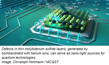
The physicists then used a layer of the semiconductor molybdenum disulfide (MoS2) as the starting material, just three atoms thick. They irradiated this with a helium ion beam which they focused on a surface area of less than one nanometer.
In order to generate optically active defects, the desired quantum light sources, molybdenum or sulfur atoms are precisely hammered out of the layer. The imperfections are traps for so-called excitons, electron-hole pairs, which then emit the desired photons.
Technically, the new helium ion microscope at the Walter Schottky Institute’s Center for Nanotechnology and Nanomaterials, which can be used to irradiate such material with an unparalleled lateral resolution, was of central importance for this.
On The Road to New Light Sources
Together with theorists at TUM, the Max Planck Society, and the University of Bremen, the team developed a model which also describes the energy states observed at the imperfections in theory.
In the future, the researchers also want to create more complex light source patterns, in lateral two-dimensional lattice structures for example, in order to thus also research multi-exciton phenomena or exotic material properties.
This is the experimental gateway to a world which has long only been described in theory within the context of the so-called Bose-Hubbard model which seeks to account for complex processes in solids.
Quantum Sensors, Transistors and Secure Encryption
And there may be progress not only in theory, but also with regard to possible technological developments. Since the light sources always have the same underlying defect in the material, they are theoretically indistinguishable. This allows for applications which are based on the quantum-mechanical principle of entanglement.
“It is possible to integrate our quantum light sources very elegantly into photon circuits,” says Klein. “Owing to the high sensitivity, for example, it is possible to build quantum sensors for smartphones and develop extremely secure encryption technologies for data transmission.”
Share on:


Subscribe
Stay ahead of the technologies shaping the future of electronics with our latest newsletter, Advanced Electronics Packaging Digest. Get expert insights on advanced packaging, materials, and system-level innovation, delivered straight to your inbox.
Subscribe now to stay informed, competitive, and connected.
Suggested Items
Green Circuits Heads to Peterson SFB to Support Next-Gen Space and Defense Electronics
05/05/2026 | Green CircuitsThe event, hosted at Peterson Space Force Base, brings together key personnel and mission partners supporting critical U.S. defense and space operations.
ASC Sunstone Circuits to Exhibit at PCB East 2026
04/26/2026 | ASC Sunstone CircuitsAnaya Vardya, President and CEO of ASC Sunstone Circuits, a leading provider of printed circuit board (PCB) fabrication and assembly solutions, announced that the company will be exhibiting at PCB East 2026, taking place April 29 at the DCU Convention Center.
Green Circuits Reports Strong Delivery and Quality Performance as Demand Scales
03/25/2026 | Green CircuitsGreen Circuits, a full-service Electronics Manufacturing Services (EMS) partner to leading OEMs, continues to deliver consistent performance across its operations, reporting a 98% average customer scorecard rating, less than 1% average RMA, and 99% on-time delivery.
China’s Top 3 FPC Manufacturers 2026: Advancing Sustainable Flexible Electronics
03/25/2026 | EINPresswire.comThe global transition towards compact, lightweight, and durable electronic devices is accelerating demand for advanced Flexible Printed Circuits (FPCs).
Elephantech Secures Mitsubishi Electric Investment to Boost SustainaCircuits Globally
03/12/2026 | ElephantechElephantech Inc. announced a strategic partnership with Mitsubishi Electric Corporation. As part of the agreement, Mitsubishi Electric will invest JPY 4 billion in Elephantech’s Series F financing.